onsemi 2SD1620
10V 3A Bipolar Transistor
| Part No. | 2SD1620 |
|---|---|
| Datasheet | 2SD1620 Download |
| Manufacturer |  onsemi |
| Description | 10V 3A Bipolar Transistor |
| Buy | Stock & Price |
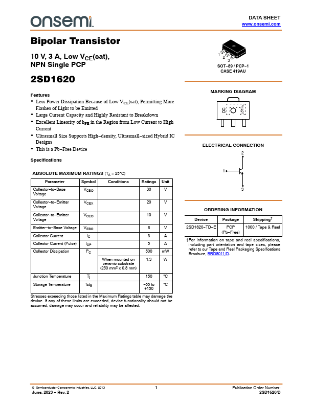
FEATURES
● Less Power Dissipation Because of Low VCE(sat), Permitting More Flashes of Light to be Emitted● Large Current Capacity and Highly Resistant to Breakdown
● Excellent Linearity of hFE in the Region from Low Current to High Current
● Ultrasmall Size Supports High−density, Ultrasmall−sized Hybrid IC Designs
● This is a Pb−Free Device Specifications
ABSOLUTE MAXIMUM RATINGS
(TA = 25C) Parameter Symbol Conditions Ratings Unit Collector−to−Base Voltage VCBO 30 V Collector−to−Emitter Voltage VCEX 20 V Collector−to−Emitter Voltage VCEO 10 V Emitter−to−Base Voltage VEBO 6 V Collector Current IC 3 A Collector Current (Pulse) ICP 5 A Collector Dissipation PC 500 mW When mounted on 1.3 W ceramic substrate (250 mm2 x 0.8 mm) Junction Temperature Tj Storage Temperature Tstg 150 C −55 to C +150 Stresses exceeding those listed in theMAXIMUM RATINGS
table may damage the device. If any of these limits are exceeded, device functionality should not be assumed, damage may occur and reliability may be affected.