DESCRIPTION
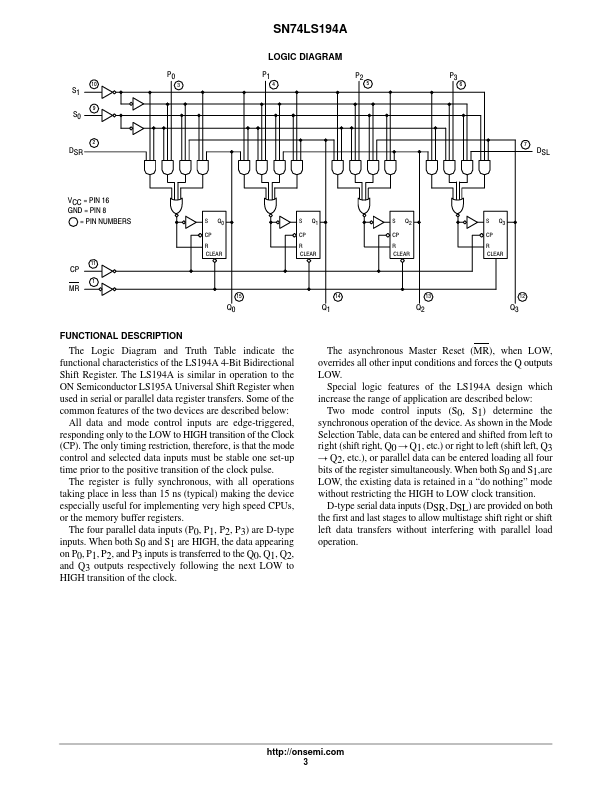
Some of the common features of the two devices are described below: All data and mode control inputs are edge-triggered, responding only to the LOW to HIGH transition of the Clock (CP). The only timing restriction, therefore, is that the mode control and selected data inputs must be stable one set-up time prior to the positive transition of the clock pulse. The register is fully synchronous, with all operations taking place in less than 15 ns (typical) making the device especially useful for implementing very high speed CPUs, or the memory buffer registers. The four parallel data inputs (P0, P1, P2, P3) are D-type inputs. When both S0 and S1 are HIGH, the data appearing on P0, P1, P2, and P3 inputs is transferred to the Q0, Q1, Q2, and Q3 outputs respectively following the next LOW to HIGH transition of the clock. The asynchronous Master Reset (MR), when LOW, overrides all other input conditions and forces the Q outputs LOW. Special logic features of the LS194A design which increase the range of application are described below: Two mode control inputs (S0, S1) determine the synchronous operation of the device. onsemi