onsemi BC637
High Current Transistors
| Part No. | BC637 |
|---|---|
| Datasheet | BC637 Download |
| Manufacturer |  onsemi |
| Description | High Current Transistors |
| Buy | Stock & Price |
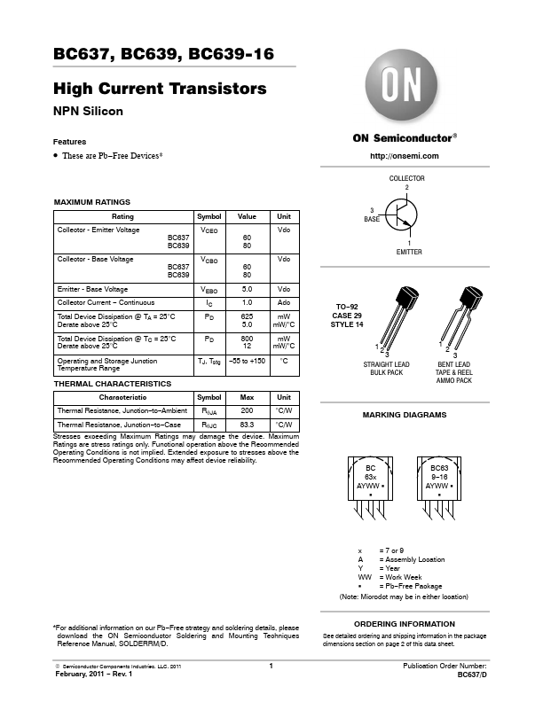
FEATURES
● These are Pb−Free Devices*MAXIMUM RATINGS
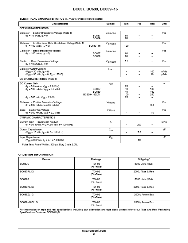
Rating Collector - Emitter Voltage Symbol BC637 BC639 VCEO Value 60 80 Unit Vdc Collector - Base Voltage BC637 BC639 VCBO 60 80 Vdc Emitter - Base Voltage Collector Current − Continuous Total Device Dissipation Derate above 25°C @ TA = 25°C VEBO IC PD 5.0 Vdc 1.0 Adc 625 mW 5.0 mW/°C Total Device Dissipation @ TC = 25°C Derate above 25°C PD 800 mW 12 mW/°C Operating and Storage Junction Temperature Range TJ, Tstg −55 to +150 °C THERMAL CHARACTERISTICS Characteristic Symbol Max Unit Thermal Resistance, Junction−to−Ambient RqJA 200 °C/W Thermal Resistance, Junction−to−Case RqJC 83.3 °C/W Stresses exceedingMAXIMUM RATINGS
may damage the device.MAXIMUM RATINGS
are stress ratings only. Functional operation above the Recommended Operating Conditions is not implied. Extended exposure to stresses above the Recommended O