onsemi BUT11AF
NPN Silicon Transistor
| Part No. | BUT11AF |
|---|---|
| Datasheet | BUT11AF Download |
| Manufacturer |  onsemi |
| Description | NPN Silicon Transistor |
| Buy | Stock & Price |
APPLICATIONS
MAXIMUM RATINGS
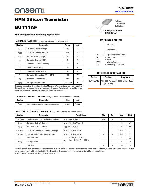
(TC = 25°C unless otherwise noted) Symbol Parameter Value Unit VCBO Collector−Base Voltage 1000 V VCEO Collector−Emitter Voltage 450 V VEBO Emitter−Base Voltage 9 V IC Collector Current (DC) 5 A ICP *Collector Current (Pulse) 10 A IB Base Current (DC) 2 A IBP *Base Current (Pulse) 4 A PC Collector Dissipation (TC = 25°C) 40 W TJ Junction Temperature 150 °C TSTG Storage Temperature −65~150 °C Stresses exceeding those listed in theMAXIMUM RATINGS
table may damage the device. If any of these limits are exceeded, device functionality should not be assumed, damage may occur and reliability may be affected. THERMAL CHARACTERISTICS (TC = 25°C, unless otherwise noted) Symbol Parameter Max Unit RqJC Thermal Resistance, Junction to Case 3.125 °C/W 1. Base 2. Collector 3. Emitter 1 TO−220 Fullpack, 3−Lead CASE 221AT MARKING DIAGRAM BUT11A F AYWWZZ BUT11AF = Specific Device Code A = Site Code Y = Year WW = Work Week ZZ = Assembly Lot Code ORDERING INFORMATION Device P...