onsemi FDMC3612
This N−Channel MOSFET is produced using onsemi’s advanced POWERTRENCH process that has been especially tailored to minimize the on−state resistance and yet maintain superior switching performance.| Part No. | FDMC3612 |
|---|---|
| Datasheet | FDMC3612 Download |
| Manufacturer |  onsemi |
| Description | N-Channel MOSFET |
| Buy | Stock & Price |
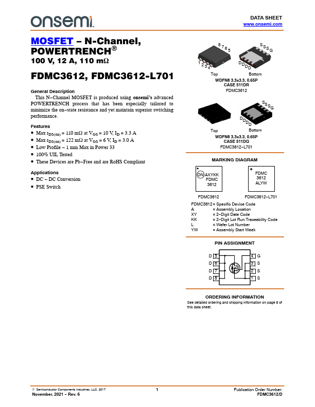
GENERAL DESCRIPTION
FEATURES
● Max rDS(on) = 110 mW at VGS = 10 V, ID = 3.3 A● Max rDS(on) = 122 mW at VGS = 6 V, ID = 3.0 A
● Low Profile − 1 mm Max in Power 33
● 100% UIL Tested
● These Devices are Pb−Free and are RoHS Compliant
APPLICATIONS
● DC − DC Conversion● PSE Switch DATA SHEET 8765 SSSG 1234 DDDD Top Bottom WDFN8 3.3x3.3, 0.65P CASE 511DR FDMC3612 SS SG DDDD Top Bottom WDFN8 3.3x3.3, 0.65P CASE 511DQ FDMC3612−L701 MARKING DIAGRAM ON AXYKK FDMC 3612 FDMC 3612 ALYW FDMC3612 FDMC3612−L701 FDMC3612 = Specific Device Code A = Assembly Location XY = 2−Digit Date Code KK = 2−Digit Lot Run Traceability Code L = Wafer Lot Number YW = Assembly Start Week PIN ASSIGNMENT D5 D6 D7 D8 4G 3S 2S 1S ORDERING INFORMATION See detailed ordering and shipping information on page 6 of this data sheet. © Semiconductor Components Industries, LLC, 2017 1 November, 2021 − Rev. 6 Publication Order Number: FDMC3612/D FDMC3612, FDMC3612−L701 MOSFET
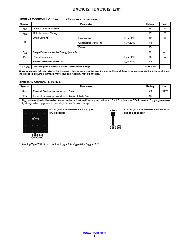
MAXIMUM RATINGS
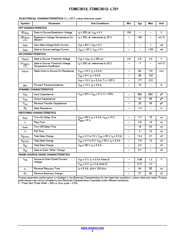
(TC = 25°C unless otherwise noted) Symb...