onsemi FDT86102LZ
This N−Channel MOSFET is produced using onsemi’s advanced POWERTRENCH process that has been especially tailored to minimize the on−state resistance and switching loss.| Part No. | FDT86102LZ |
|---|---|
| Datasheet | FDT86102LZ Download |
| Manufacturer |  onsemi |
| Description | N-Channel MOSFET |
| Buy | Stock & Price |
GENERAL DESCRIPTION
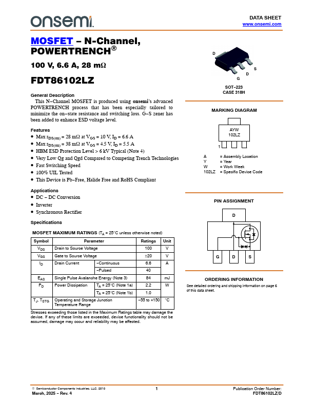
G−S zener has been added to enhance ESD voltage level. S D G SOT−223 CASE 318H MARKING DIAGRAMFEATURES
● Max rDS(on) = 28 mW at VGS = 10 V, ID = 6.6 A● Max rDS(on) = 38 mW at VGS = 4.5 V, ID = 5.5 A
● HBM ESD Protection Level > 6 kV Typical (Note 4)
● Very Low Qg and Qgd Compared to Competing Trench Technologies
● Fast Switching Speed
● 100% UIL Tested
● This Device is Pb−Free, Halide Free and RoHS Compliant AYW 102LZ 1 A Y W 102LZ = Assembly Location = Year = Work Week = Specific Device Code
APPLICATIONS
● DC − DC Conversion● Inverter
● Synchronous Rectifier Specifications PIN ASSIGNMENT D MOSFET
MAXIMUM RATINGS
(TA = 25°C unless otherwise noted) Symbol Parameter Ratings Unit VDS Drain to Source Voltage VGS Gate to Source Voltage ID Drain Current −Continuous −Pulsed 100 V ±20 V 6.6 A 40 EAS PD TJ, TSTG Single Pulse Avalanche Energy (Note 3) Power Dissipation TA = 25°C (Note 1a) TA = 25°C (Note 1b) Operating and Storage Junction Temperature Range 84 mJ 2.2 W 1.0 −55 to +150 °C Stresses exceeding those listed in theMAXIMUM RATINGS
table may damage the device.
