ACE2607B Description
ACE2607B is produced with high cell density, DMOS trench technology, which is especially used to minimize on-state resistance. This device particularly suits for low voltage application such as portable equipment, power management and other battery powered circuits, and low in-line power loss are needed in a very small outline surface mount package.
ACE2607B Key Features
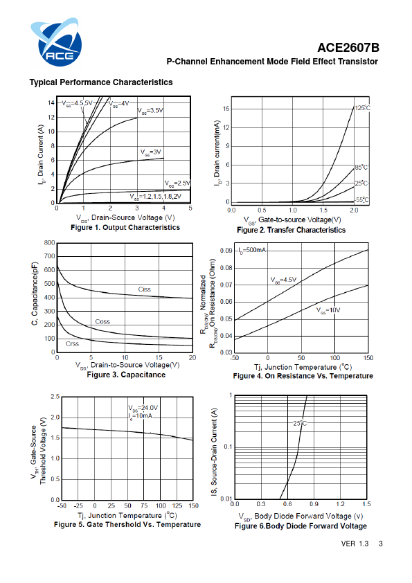
- VDS(V)=-30V, ID=-3.5A
- RDS(ON)=52mΩ@VGS=-10V
- RDS(ON)=68mΩ@VGS=-4.5V
- High density cell design for low RDS(ON)