Datasheet4U Logo Datasheet4U.com

ACE2301 - P-Channel Enhancement Mode MOSFET

General Description

The ACE2301 is the P-Channel logic enhancement mode power field effect transistor are produced using high cell density, DMOS trench technology.

This high density process is especially tailored to minimize on-state resistance.

Key Features

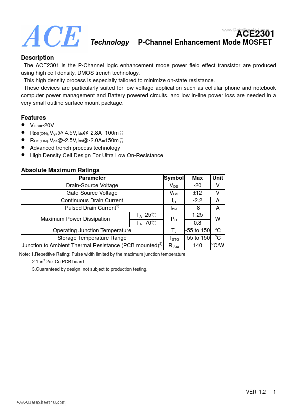
  • VDS=-20V RDS(ON),Vgs@-4.5V,Ids@-2.8A=100mΩ RDS(ON),Vgs@-2.5V,Ids@-2.0A=150mΩ Advanced trench process technology High Density Cell Design For Ultra Low On-Resistance Absolute Maximum Ratings Parameter Drain-Source Voltage Gate-Source Voltage Continuous Drain Current Pulsed Drain Current1) Maximum Power Dissipation TA=25℃ TA=70℃ Symbol VDS VGS ID IDM PD TJ TSTG RθJA Max Unit -20 V ±12 V -2.2 A -8 A 1.25 W 0.8 -55 to 150 OC -55 to 150 OC O 140 C/.

📥 Download Datasheet

Datasheet Details

Part number ACE2301
Manufacturer ACE Technology
File Size 114.79 KB
Description P-Channel Enhancement Mode MOSFET
Datasheet download datasheet ACE2301 Datasheet

Full PDF Text Transcription (Reference)

The following content is an automatically extracted verbatim text from the original manufacturer datasheet and is provided for reference purposes only.

View original datasheet text
www.DataSheet4U.com ACE2301 Technology Description P-Channel Enhancement Mode MOSFET The ACE2301 is the P-Channel logic enhancement mode power field effect transistor are produced using high cell density, DMOS trench technology. This high density process is especially tailored to minimize on-state resistance. These devices are particularly suited for low voltage application such as cellular phone and notebook computer power management and Battery powered circuits, and low in-line power loss are needed in a very small outline surface mount package. Features • • • • • VDS=-20V RDS(ON),Vgs@-4.5V,Ids@-2.8A=100mΩ RDS(ON),Vgs@-2.5V,Ids@-2.