SSC8329GS1 Description
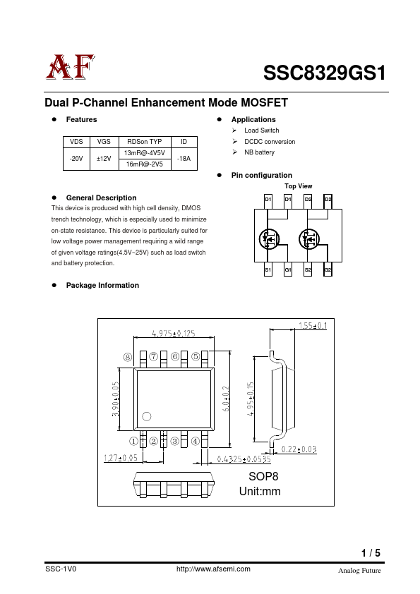
This device is produced with high cell density, DMOS Top View D1 D1 D2 trench technology, which is especially used to minimize on-state resistance. This device is particularly suited for low voltage power management requiring a wild range of given voltage ratings(4.5V~25V) such as load switch and battery protection. S1 G1 S2 Package Information D2 G2 ⑧ ⑦ ⑥⑤ ①② ③ ④ SOP8 Unit:mm SSC-1V0 http://.afsemi.


