Datasheet Summary
..
A67P06181/A67P93361 Series
Preliminary
Document Title 1M X 18, 512K X 36 LVTTL, Flow-through ZeBLTM SRAM Revision History
Rev. No.
1M X 18, 512K X 36 LVTTL, Flow-through ZeBLTM SRAM
History
Initial issue
Issue Date
September, 20, 2004
Remark
Preliminary
PRELIMINARY
(September, 2004, Version 0.0)
AMIC Technology, Corp.
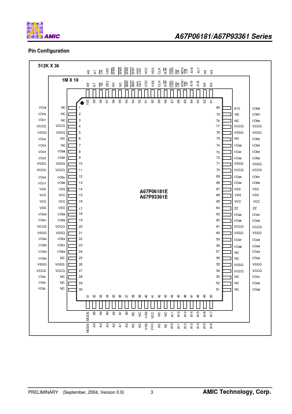
A67P06181/A67P93361 Series
Preliminary
Features
Fast access time: 6.5/7.5/8.5 ns (153, 133, 117 MHz) Zero Bus Latency between READ and WRITE cycles allows 100% bus utilization Signal +2.5V ± 5% power supply Individual Byte Write control capability Clock enable ( CEN ) pin to enable clock and suspend operations Clock-controlled and registered...