AAT9512 Overview
Description
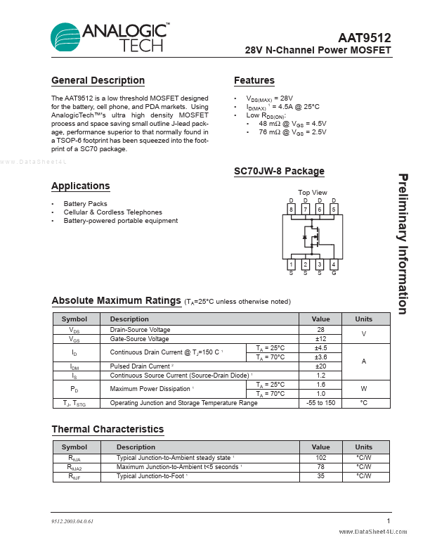
Drain-Source Voltage Gate-Source Voltage Continuous Drain Current @ TJ=150 C 1 Units V TA = 25°C TA = 70°C 1 Pulsed Drain Current 2 Continuous Source Current (Source-Drain Diode) Maximum Power Dissipation 1 A TA = 25°C TA = 70°C Operating Junction and Storage Temperature Range W °C Symbol RθJA RθJA2 RθJF Description Typical Junction-to-Ambient steady state Maximum Junction-to-Ambient t<5 seconds Typical Junction-to-Foot 1 1 1 Value 102 78 35 Units °C/W °C/W °C/W 9512.2003.04.0.61 1 28V N-Channel Power MOSFET Symbol Description (TJ=25°C unless otherwise noted) Conditions Min 28 36 57 20 0.6 ±100 1 5 7 5 0.9 1 6 3 30 8 1.6 1.2 48 76 AAT9512 Typ Max Units V mΩ A V nA µA S DC Characteristics BVDSS Drain-Source Breakdown Voltage VGS=0V, ID=250µA VGS=4.5V, ID=4.5A RDS(ON) Drain-Source ON-Resistance 2 VGS=2.5V, ID=3.6A ID(ON) On-State Drain Current 2 VGS=4.5V, VDS=5V (Pulsed) VGS(th) Gate Threshold Voltage VGS=VDS, ID=250µA IGSS Gate-Body Leakage Current VGS=±12V, VDS=0V VGS=0V, VDS=28V IDSS Drain Source.
Key Features
- VDS(MAX) = 28V ID(MAX) 1 = 4.5A @ 25°C Low RDS(ON)
- 48 mΩ @ VGS = 4.5V
- 76 mΩ @ VGS = 2.5V SC70JW-8 Package Applications