Datasheet Summary
$XJXVW
- $6&0(
9 0î &026 '5$0 ('2 )HDWXUHV
- Organization: 1,048,576 words × 16 bits
- High speed
- 45/50/60 ns RAS access time
- 20/20/25 ns hyper page cycle time
- 10/12/15 ns CAS access time
- 1024 refresh cycles, 16 ms refresh interval
- RAS-only or CAS-before-RAS refresh Read-modify-write
- TTL-patible, three-state DQ
- JEDEC standard package and pinout
- 400 mil, 42-pin SOJ
- 400 mil, 44/50-pin TSOP 2
- Low power consumption
- Active: 740 mW max (AS4C1M16E5-60)
- Standby: 5.5 mW max, CMOS DQ
- 5V power supply
- Industrial and mercial temperature available
- Extended data out
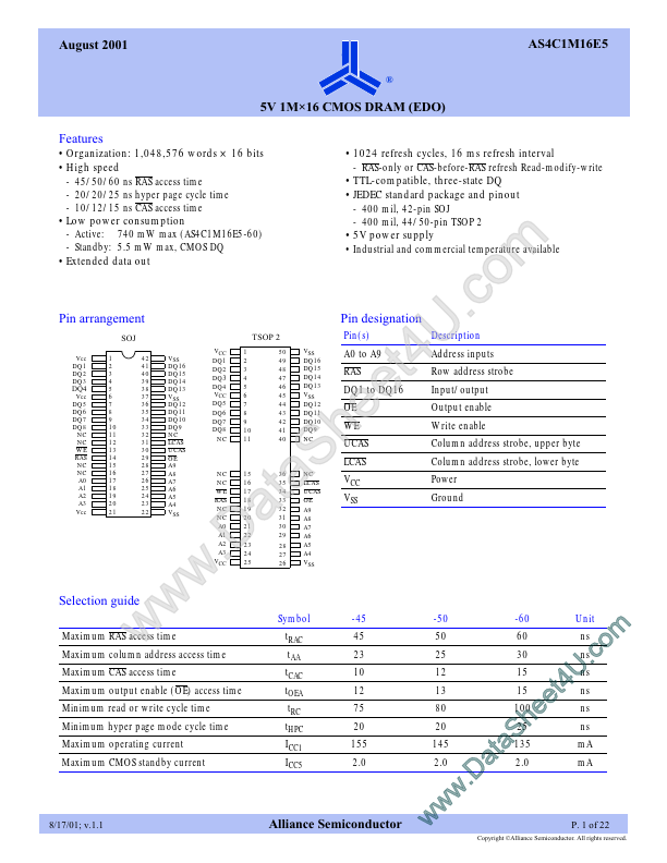
3LQ DUUDQJHPHQW
62Vcc DQ1 DQ2 DQ3 '4 Vcc DQ5 DQ6 DQ7 DQ8 NC NC WE RAS NC NC A0...