Datasheet Details
| Part number | AOD607A |
|---|---|
| Manufacturer | Alpha & Omega Semiconductors |
| File Size | 563.13 KB |
| Description | 30V Complementary MOSFET |
| Download | AOD607A Download (PDF) |
|
|
| Part number | AOD607A |
|---|---|
| Manufacturer | Alpha & Omega Semiconductors |
| File Size | 563.13 KB |
| Description | 30V Complementary MOSFET |
| Download | AOD607A Download (PDF) |
|
|
|
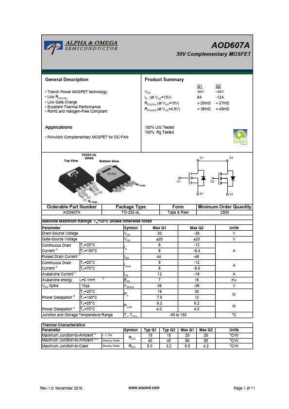
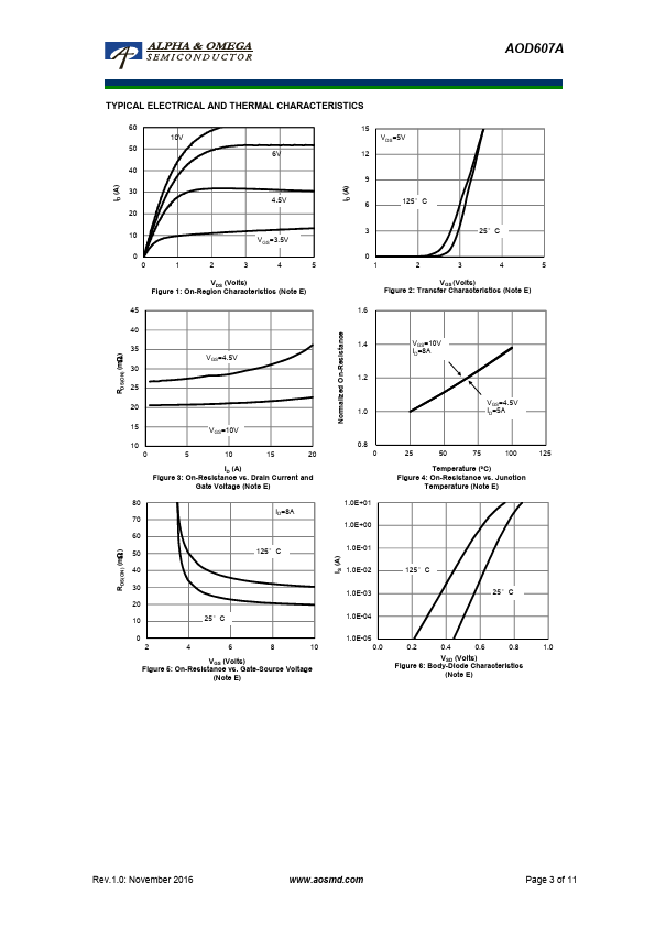
• Trench Power MOSFET technology • Low RDS(ON) • Low Gate Charge • Excellent Thermal Performance • RoHS and Halogen-Free Compliant Applications • Pch+Nch Complementary MOSFET for DC-FAN Product Summary VDS ID (at VGS=10V) RDS(ON) (at VGS=10V) RDS(ON) (at VGS=4.5V) Q1 30V 8A < 25mΩ < 38mΩ Q2 -30V -12A < 27mΩ < 45mΩ 100% UIS Tested 100% Rg Tested TO252-4L Top View DPAK Bottom View D1 D2 D1/D2 D1/D2 S2 G2 S1G1 PIN1 Orderable Part Number AOD607A PIN1 Package Type TO-252-4L G1 G2 S1 S2 Form Tape & Reel Minimum Order Quantity 2500 Absolute Maximum Ratings TA=25°C unless otherwise noted Parameter Symbol Max Q1 Drain-Source Voltage VDS 30 Gate-Source Voltage VGS ±20 Continuous Drain Current G TC=25°C TC=100°C ID 8 8 Pulsed Drain Current C IDM 44 Continuous Drain Current G TA=25°C TA=70°C 8 IDSM 8 Avalanche Current C IAS 12 Avalanche energy L=0.1mH C EAS 7 VDS Spike Power Dissipation B 10µs TC=25°C TC=100°C VSPIKE 36 19 PD 7.5 TA=25°C Power Dissipation A TA=70°C 6.2 PDSM 4.0 Junction and Storage Temperature Range TJ, TSTG -55 to 150 Max Q2 -30 ±20 -12 -9.4 -48 -12 -9.5 -18 16 -36 30 12 6.2 4.0 Units V V A A A mJ V W W °C Thermal Characteristics Parameter Maximum Junction-to-Ambient A Maximum Junction-to-Ambient A D Maximum Junction-to-Case t ≤ 10s Steady-State Steady-State Symbol RθJA RθJC Typ Q1 15 40 5.0 Typ Q2 15 40 3.2 Max Q1 20 50 6.5 Max Q2 20 50 4.2 Units °C/W °C/W °C/W Rev.1.0: November 2016 www.aosmd.com Page 1 of 11 AOD607A Q1 Electrical Characteristics (TJ=25°C unless otherwise noted) Symbol Parameter Conditions Min STATIC PARAMETERS BVDSS Drain-Source Breakdown Voltage ID=250µA, VGS=0V 30 IDSS Zero Gate Voltage Drain Current VDS=30V, VGS=0V TJ=55°C IGSS Gate-Body leakage current VDS=0V, VGS=±20V VGS(th) Gate Threshold Voltage VDS=VGS, ID=250µA 1.5 VGS=10V, ID=8A RDS(ON) Static Drain-Source On-Resistance TJ=125°C VGS
AOD607A 30V Complementary MOSFET General.
| Part Number | Description |
|---|---|
| AOD607 | MOSFET |
| AOD600A70 | 700V N-Channel Power Transistor |
| AOD600A70P | N-Channel Power Transistor |
| AOD600A70R | N-Channel Power Transistor |
| AOD603 | MOSFET |
| AOD603A | 60V Complementary MOSFET |
| AOD604 | MOSFET |
| AOD606 | MOSFET |
| AOD609 | 40V Complementary MOSFET |
| AOD609G | Complementary Enhancement Mode Field Effect Transistor |