AOT9N40
AOT9N40 is N-Channel MOSFET manufactured by Alpha & Omega Semiconductors.
400V,8A N-Channel MOSFET
General Description
Product Summary
The AOT9N40 is fabricated using an advanced high voltage MOSFET process that is designed to deliver high levels of performance and robustness in popular AC-DC applications.By providing low RDS(on), Ciss and Crss along with guaranteed avalanche capability this parts can be adopted quickly into new and existing offline power supply designs.These parts are ideal for boost converters and synchronous rectifiers for consumer, tele, industrial power supplies and LED backlighting.
VDS ID (at VGS=10V) RDS(ON) (at VGS=10V)
100% UIS Tested 100% Rg Tested
For Halogen Free add "L" suffix to part number: AOT9N40L
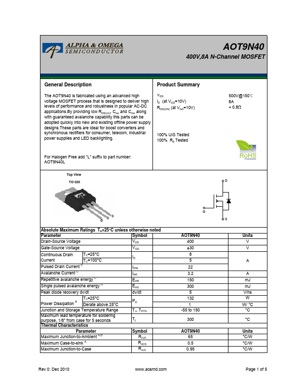
Top View TO-220
500V@150℃ 8A < 0.8Ω
DS...