Datasheet Details
| Part number | AOU7S65 |
|---|---|
| Manufacturer | Alpha & Omega Semiconductors |
| File Size | 354.54 KB |
| Description | Power Transistor |
| Datasheet |
 AOU7S65 Datasheet AOU7S65 Datasheet
|
|
|
| Part number | AOU7S65 |
|---|---|
| Manufacturer | Alpha & Omega Semiconductors |
| File Size | 354.54 KB |
| Description | Power Transistor |
| Datasheet |
AOU7S65 Datasheet
|
|
|
|
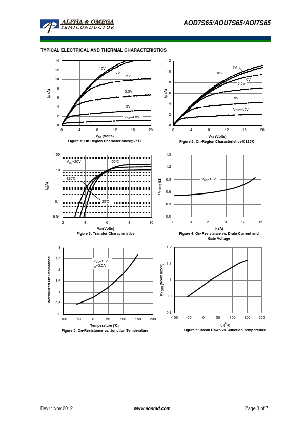
Product Summary The AOD7S65 & AOU7S65 & AOI7S65 have been fabricated using the advanced αMOSTM high voltage process that is designed to deliver high levels of performance and robustness in switching applications.
By providing low RDS(on), Qg and EOSS along with guaranteed avalanche capability these parts can be adopted quickly into new and existing offline power supply designs.
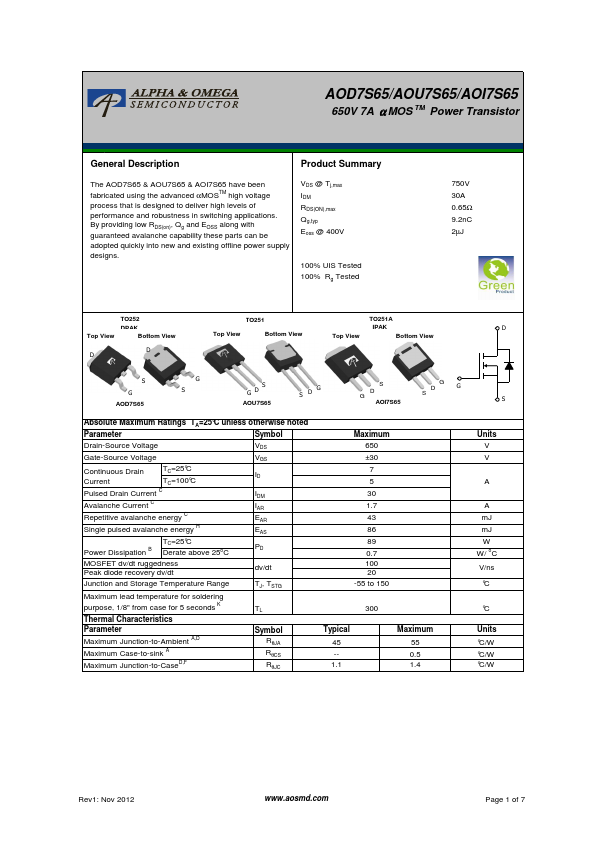
VDS @ Tj,max IDM RDS(ON),max Qg,typ Eoss @ 400V 100% UIS Tested 100% Rg Tested 750V 30A 0.65Ω 9.2nC 2µJ TO252 DPAK Top View Bottom View D D TO251 Top View Bottom View Top View TO251A IPAK Bottom View D S G AOD7S65 G S S GD AOU7S65 G SD S D G AOI7S65 G D S G Absolute Maximum Ratings TA=25°C unless otherwise noted Parameter Symbol Drain-Source Voltage VDS Gate-Source Voltage VGS Continuous Drain TC=25°C Current TC=100°C Pulsed Drain Current C Avalanche Current C Repetitive avalanche energy C Single pulsed avalanche energy H ID IDM IAR EAR EAS TC=25°C Power Dissipation B Derate above 25oC PD MOSFET dv/dt ruggedness Peak diode recovery dv/dt dv/dt Junction and Storage Temperature Range TJ, TSTG Maximum lead temperature for soldering purpose, 1/8" from case for 5 seconds K Thermal Characteristics TL Parameter Maximum Junction-to-Ambient A,D Maximum Case-to-sink A Maximum Junction-to-CaseD,F Symbol RθJA RθCS RθJC Maximum 650 ±30 7 5 30 1.7 43 86 89 0.7 100 20 -55 to 150 300 Typical 45 -1.1 Maximum 55 0.5 1.4 S Units V V A A mJ mJ W W/ oC V/ns °C °C Units °C/W °C/W °C/W Rev1: Nov 2012 www.aosmd.com Page 1 of 7 AOD7S65/AOU7S65/AOI7S65 Electrical Characteristics (TJ=25°C unless otherwise noted) Symbol Parameter Conditions STATIC PARAMETERS BVDSS Drain-Source Breakdown Voltage ID=250µA, VGS=0V, TJ=25°C ID=250µA, VGS=0V, TJ=150°C IDSS Zero Gate Voltage Drain Current VDS=650V, VGS=0V VDS=520V, TJ=150°C IGSS Gate-Body leakage current VDS=0V, VGS=±30V VGS(th) Ga
AOD7S65/AOU7S65/AOI7S65 650V 7A α MOS TM Power Transistor General.
| Brand Logo | Part Number | Description | Manufacturer |
|---|---|---|---|
| AOU7S65 | N-Channel MOSFET | INCHANGE |
| Part Number | Description |
|---|---|
| AOU7S60 | Power Transistor |
| AOU1N60 | 1.3A N-Channel MOSFET |
| AOU2N60 | 2A N-Channel MOSFET |
| AOU2N60A | 2A N-Channel MOSFET |
| AOU3N50 | 500V 3A N-Channel MOSFET |
| AOU3N60 | N-Channel MOSFET |
| AOU400 | N-Channel MOSFET |
| AOU401 | P-Channel MOSFET |
| AOU402 | N-Channel MOSFET |
| AOU403 | P-Channel MOSFET |