ADN4664 Description
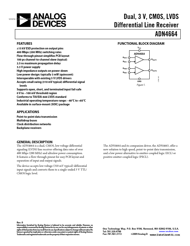
The ADN4664 is a dual, CMOS, low voltage differential signaling (LVDS) line receiver offering data rates of over 400 Mbps (200 MHz) and ultralow power consumption.
| Part number | ADN4664 |
|---|---|
| Download | ADN4664 Datasheet (PDF) |
| File Size | 348.47 KB |
| Manufacturer | Analog Devices |
| Description | LVDS Differential Line Receiver |
|
|
| Part Number | Description |
|---|---|
| ADN4661 | High Speed Differential Driver |
| ADN4662 | LVDS Differential Line Receiver |
| ADN4663 | LVDS High Speed Differential Driver |
| ADN4665 | CMOS Differential Line Driver |
| ADN4666 | Quad CMOS Differential Line Receiver |
The ADN4664 is a dual, CMOS, low voltage differential signaling (LVDS) line receiver offering data rates of over 400 Mbps (200 MHz) and ultralow power consumption.