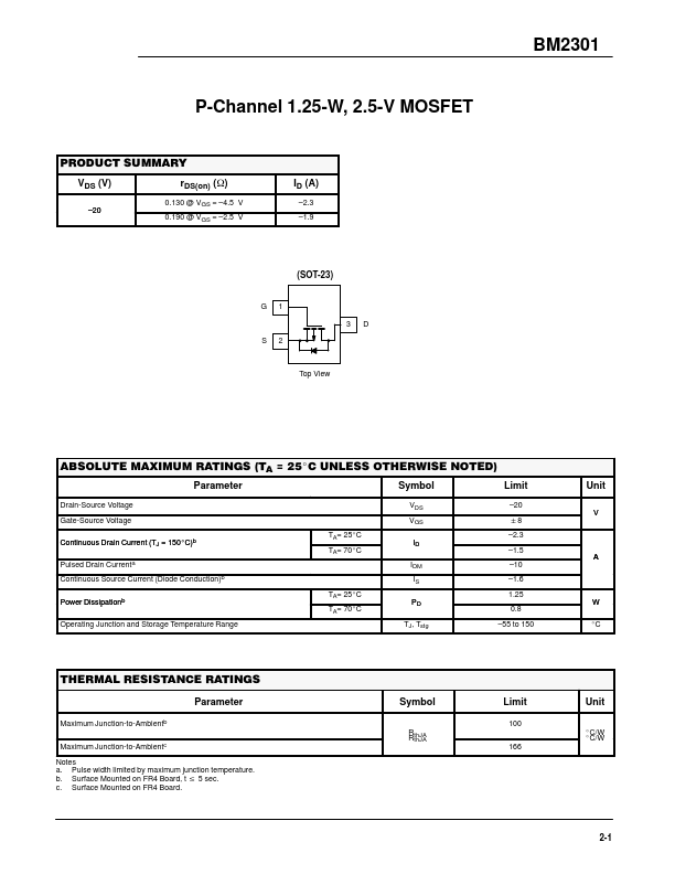
BM2301 Description
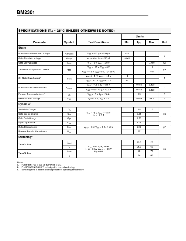
Pulse width limited by maximum junction temperature. Surface Mounted on FR4 Board, t v 5 sec. Surface Mounted on FR4 Board.
BM2301 is P-Channel MOSFET manufactured by Bookly.
| Part Number | Description |
|---|---|
| BM2300 | N-Channel Enhancement Mode MOSFET |
| BM2302 | N-Channel MOSFET |
| BM2341 | P-Channel Enhancement Mode MOSFET |
| BM2262 | Remote control coding IC |
| BM2490 | 2.5A CC or CV BUCK |
Pulse width limited by maximum junction temperature. Surface Mounted on FR4 Board, t v 5 sec. Surface Mounted on FR4 Board.