CP716V Description
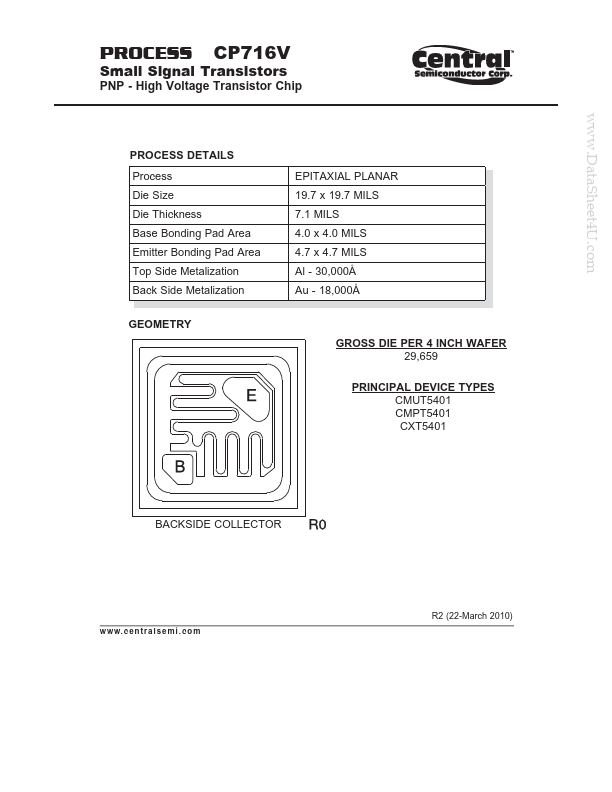
PROCESS Small Signal Transistors CP716V PNP - High Voltage Transistor Chip .. c o m PROCESS CP716V Typical R2 (22-March 2010) w w.
CP716V Key Features
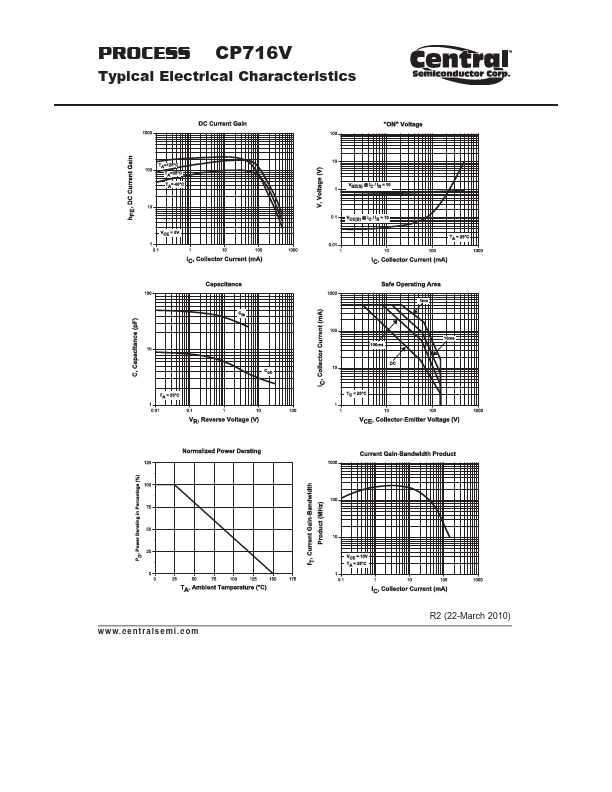
- s e m i . c o m PROCESS CP716V Typical
CP716V is PNP Transistor manufactured by Central Semiconductor.
| Part Number | Description |
|---|---|
| CP716 | PNP Transistor |
| CP710 | PNP Transistor |
| CP710V | PNP Transistor |
| CP712 | PNP Transistor |
| CP714 | PNP Transistor |
PROCESS Small Signal Transistors CP716V PNP - High Voltage Transistor Chip .. c o m PROCESS CP716V Typical R2 (22-March 2010) w w.