CY24272 Description
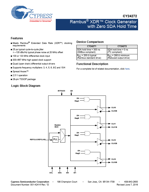
For a plete list of related documentation, click here. Logic Block Diagram /BYPASS EN Bypass MUX REFCLK,REFCLKB PLL EN RegA EN RegB EN RegC CLK0 CLK0B CLK1 CLK1B CLK2 CLK2B EN RegD CLK3 CLK3B SCL SDA.
CY24272 Key Features
- Meets Rambus® Extended Data Rate (XDR™) clocking requirements
- 25 ps typical cycle-to-cycle jitter
- 135 dBc/Hz typical phase noise at 20 MHz offset
- 100 or 133 MHz differential clock input
- 300-667 MHz high speed clock support
- Quad (open drain) differential output drivers
- Supports frequency multipliers: 3, 4, 5, 6, 9/2 and 15/4
- Spread Aware™
- 2.5 V operation
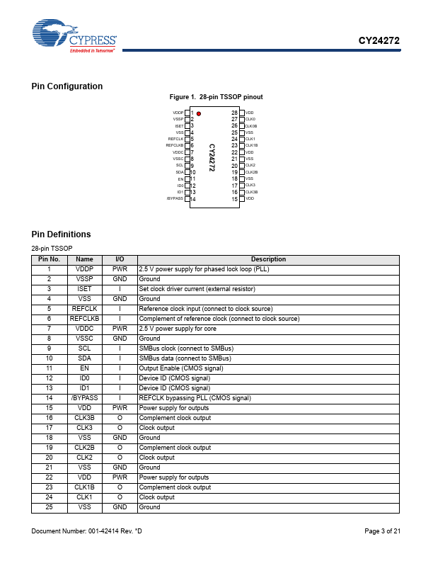
- 28-pin TSSOP package