CY24239
CY24239 is Spread Spectrum Frequency Timing Generator manufactured by Cypress.
..
Spread Spectrum Frequency Timing Generator
Features
- Maximized EMI Suppression using Cypress’s Spread Spectrum Technology
- - 1.2% and
- 2.4% Spread Spectrum support
- Three copies of CPU output
- Seven copies of PCI output
- One 48-MHz output for USB / One 24-MHz for SIO
- Two buffered reference outputs
- Two IOAPIC outputs
- Seventeen SDRAM outputs provide support for 4 DIMMs
- SMBus interface for programming
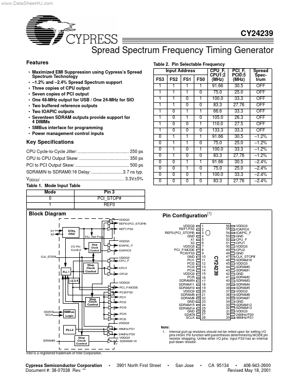
- Power management control inputs Table 2. Pin Selectable Frequency Input Address CPU_F, CPU1:2 FS3 FS2 FS1 FS0 (MHz) 1 1 1 1 91.66 1 1 1 0 75.0 1 1 0 1 100.0 1 1 0 0 83.3 1 0 1 1 66.6 1 0 1 0 105.0 1 0 0 1 110.0 1 0 0 0 133.3 0 1 1 1 91.66 0 1 1 0 75.0 0 1 0 1 100.0 0 1 0 0 83.3 0 0 1 1 91.66 0 0 1 0 75.0 0 0 0 1 100.0 0 0 0 0 83.3 PCI_F, PCI0:5 (MHz) 30.5 25.0 33.3 27.76 33.3 26.3 27.5 33.3 30.5 25.0 33.3 27.76 30.5 25.0 33.3 27.76 Spread Spectrum OFF OFF OFF OFF OFF OFF OFF OFF
- 1.2%
- 1.2%
- 1.2%
- 1.2%
- 2.4%
- 2.4%
- 2.4%
- 2.4%
Key Specifications
CPU Cycle-to-Cycle Jitter: .......................................... 250 ps CPU to CPU Output Skew: ......................................... 350 ps PCI to PCI Output Skew: ............................................ 500 ps SDRAMIN to SDRAM0:16 Delay: ..........................3.7 ns typ. VDDQ3: .................................................................... 3.3V±5% Table 1. Mode Input Table Mode 0 1 Pin 3 PCI_STOP# REF0
Block Diagram
VDDQ3 REF0/(PCI_STOP#) X1 X2 XTAL OSC REF1/FS2 PLL Ref Freq
Stop Clock Control
Pin Configuration[1]
VDDQ3 REF1/FS2 REF0/(PCI_STOP#) GND X1 X2 VDDQ3 PCI_F/MODE PCI0/FS3 GND PCI1 PCI2 PCI3 PCI4 VDDQ3 PCI5 SDRAMIN SDRAM11 SDRAM10 VDDQ3 SDRAM9 SDRAM8 GND SDRAM15 SDRAM14 GND SDATA SCLK 1 2 3 4 5 6 7 8 9 10 11 12 13 14 15 16 17 18 19 20 21 22 23 24 25 26 27 28 56 55 54 53 52 51 50 49 48 47 46 45 44 43 42 41 40 39 38 37 36 35 34 33 32 31 30 29 VDDQ3 IOAPIC0 IOAPIC_F GND CPU_F CPU1 VDDQ3 CPU2 GND CLK_STOP# SDRAM16 VDDQ3 SDRAM0 SDRAM1 GND SDRAM2 SDRAM3...