CY24272 Overview
Key Specifications
Package: TSSOP
Pins: 28
Operating Voltage: 2.5 V
Max Voltage (typical range): 2.625 V
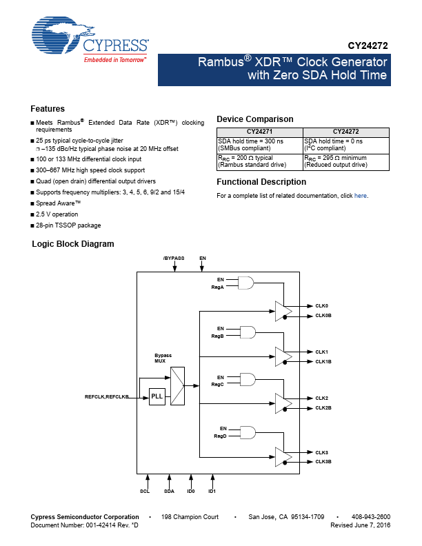
Key Features
- Meets Rambus® Extended Data Rate (XDR™) clocking requirements
- 25 ps typical cycle-to-cycle jitter ❐ –135 dBc/Hz typical phase noise at 20 MHz offset
- 100 or 133 MHz differential clock input
- 300–667 MHz high speed clock support
- Quad (open drain) differential output drivers