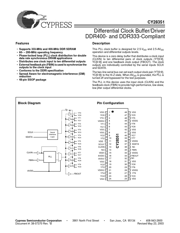
CY28351 Key Features
- Supports 333-MHz and 400-MHz DDR SDRAM
- 200-MHz operating frequency
- Phase-locked loop (PLL) clock distribution for double data rate synchronous DRAM
| Part Number | Description |
|---|---|
| CY28352 | Differential Clock Buffer/Driver |
| CY28354-400 | 210-MHz 24-Output Buffer |
| CY28358 | 200-MHz Differential Clock Buffer/Driver |
| CY28359 | 273-MHz 6-Output Buffer |
| CY28301 | Frequency Generator for Intel Integrated Chipset |