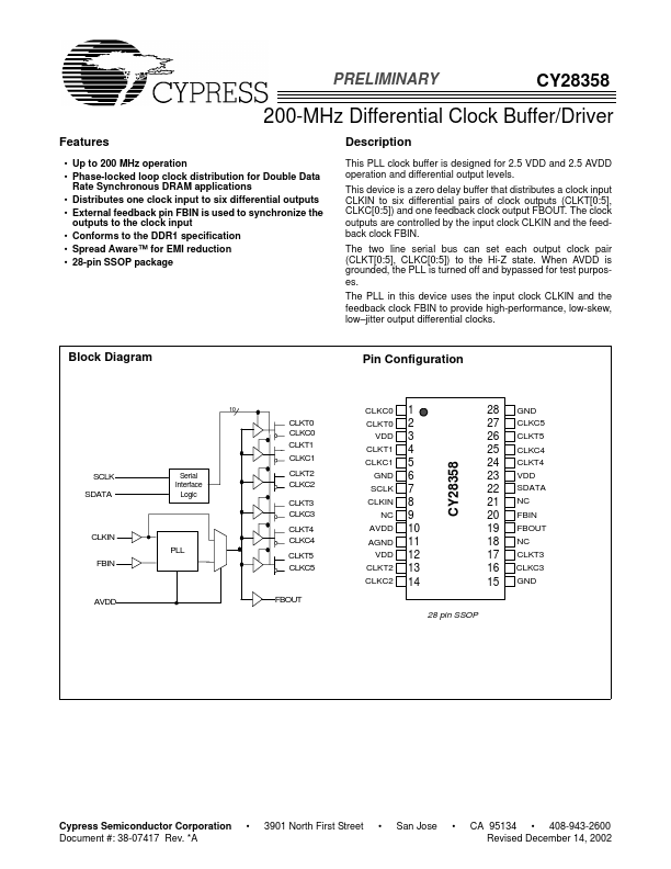
CY28358 Key Features
- Up to 200 MHz operation
- Phase-locked loop clock distribution for Double Data Rate Synchronous DRAM
| Part Number | Description |
|---|---|
| CY28351 | Differential Clock Buffer/Driver |
| CY28352 | Differential Clock Buffer/Driver |
| CY28354-400 | 210-MHz 24-Output Buffer |
| CY28359 | 273-MHz 6-Output Buffer |
| CY28301 | Frequency Generator for Intel Integrated Chipset |