CY28351
CY28351 is Differential Clock Buffer/Driver manufactured by Cypress.
Features
- Supports 333-MHz and 400-MHz DDR SDRAM
- 60-
- 200-MHz operating frequency
- Phase-locked loop (PLL) clock distribution for double data rate synchronous DRAM applications
- Distributes one clock input to ten differential outputs
- External feedback pin (FBIN) is used to synchronize the outputs to the clock input
- Conforms to the DDRI specification
- Spread Aware for electromagnetic interference (EMI) reduction
- 48-pin SSOP package
Description
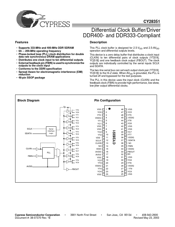
This PLL clock buffer is designed for 2.5-VDD and 2.5-AVDD operation and differential outputs levels. This device is a zero delay buffer that distributes a clock input (CLKIN) to ten differential pairs of clock outputs (YT[0:9], YC[0:9]) and one feedback clock output (FBOUT). The clock outputs are individually controlled by the serial inputs SCLK and SDATA. The two-line serial bus can set each output clock pair (YT[0:9], YC[0:9]) to the Hi-Z state. When AVDD is grounded, the PLL is turned off and bypassed for the test purposes. The PLL in this device uses the input clock (CLKIN) and the feedback clock (FBIN) to provide high-performance, low-skew, low-jitter output differential clocks.
Block Diagram
Pin Configuration
YT0 YC0 YT1 YC1 YT2 YC2
SCLK SDATA
YT4 YC4 YT5 YC5 YT6 YC6
CLKIN PLL FBIN
YT7 YC7 YT8 YC8 YT9 YC9
Serial Interface Logic
YT3 YC3
AVDD FBOUT
VSS YC0 YT0 VDDQ YT1 YC1 VSS VSS YC2 YT2 VDD SCLK CLKIN NC VDDI AVDD AVSS VSS YC3 YT3 VDDQ YT4 YC4 VSS
1 2 3 4 5 6 7 8 9 10 11 12 13 14 15 16 17 18 19 20 21 22 23 24
48 47 46 45 44 43 42 41 40 39 38 37 36 35 34 33 32 31 30 29 28 27 26 25
VSS YC5 YT5 VDDQ YT6 YC6 VSS VSS YC7 YT7 VDDQ SDATA NC FBIN VDDQ FBOUT NC VSS YC8 YT8 VDDQ YT9 YC9 VSS
Cypress Semiconductor Corporation Document #: 38-07370 Rev.
- B
- 3901 North First Street
- San Jose, CA 95134
- 408-943-2600 Revised May 23, 2003
Pin Description
[1]
Pin Number 13 35 3, 5, 10, 20, 22 46, 44, 39, 29, 27 2, 6, 9, 19, 23 47, 43, 40, 30, 26 33 Pin Name CLKIN FBIN YT(0:9) YC(0:9)...