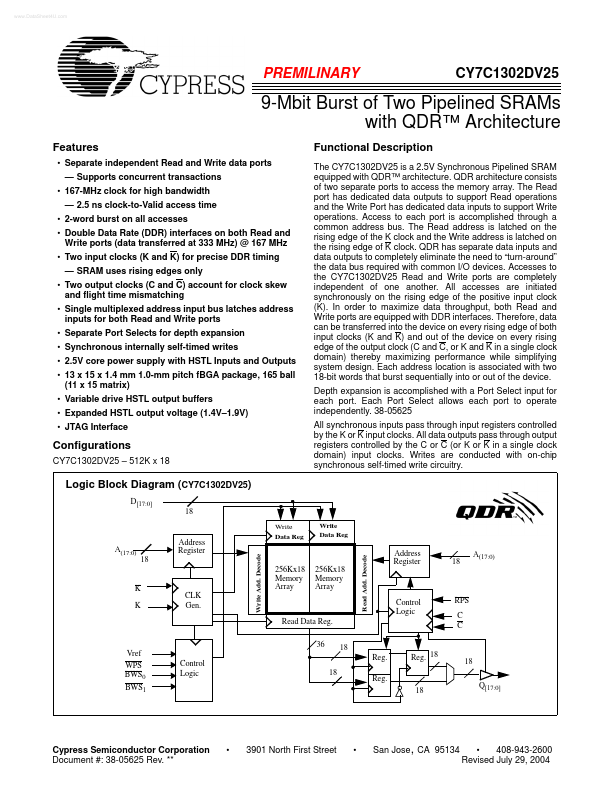
CY7C1302DV25 Overview
Key Specifications
Package: FBGA
Mount Type: Surface Mount
Pins: 165
Operating Voltage: 2.5 V
Key Features
- Separate independent Read and Write data ports
- Supports concurrent transactions
- 167-MHz clock for high bandwidth
- 2.5 ns clock-to-Valid access time
- 2-word burst on all accesses