Part number:
CY7C286
Manufacturer:
Cypress Semiconductor
File Size:
208.87 KB
Description:
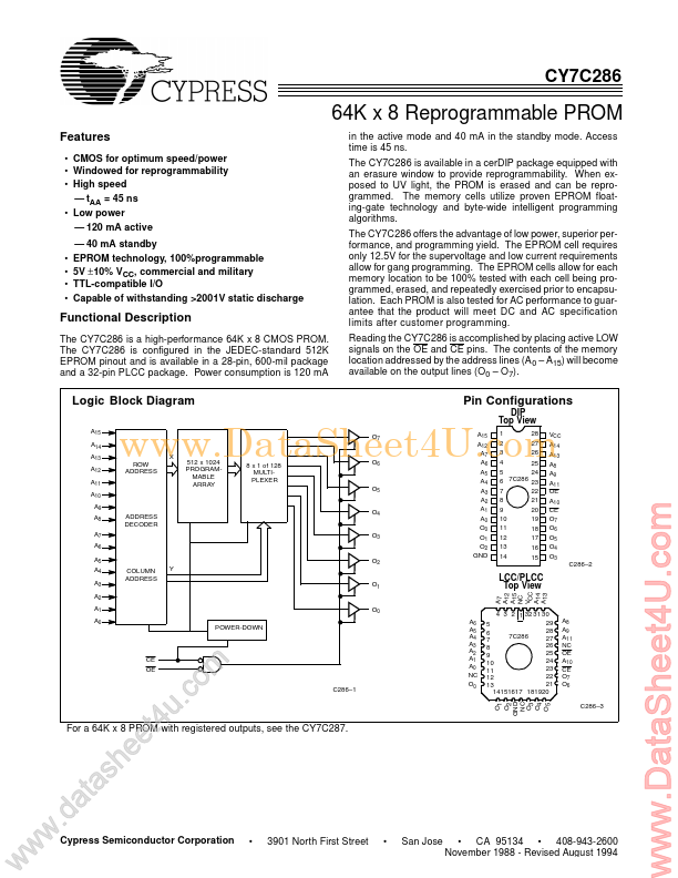
64k x 8 prom.
CY7C286 Features
* CMOS for optimum speed/power
* Windowed for reprogrammability
* High speed
* tAA = 45 ns
* Low power
* 120 mA active
* 40 mA standby EPROM technology, 100%programmable 5V ±10% VCC, commercial and milita
CY7C286_CypressSemiconductor.pdf
Datasheet Details
CY7C286
Cypress Semiconductor
208.87 KB
64k x 8 prom.
📁 Related Datasheet
CY7C281 (CY7C281 / CY7C282) 1K x 8 PROM (Cypress Semiconductor)
CY7C281A (CY7C281A / CY7C282A) 1K x 8 PROM (Cypress Semiconductor)
CY7C282 (CY7C281 / CY7C282) 1K x 8 PROM (Cypress Semiconductor)
CY7C282A (CY7C281A / CY7C282A) 1K x 8 PROM (Cypress Semiconductor)
CY7C285 64K x 8 PROM (Cypress Semiconductor)
CY7C2163KV18 18-Mbit QDR II+ SRAM Four-Word Burst Architecture (Cypress Semiconductor)
CY7C2165KV18 18-Mbit QDR II+ SRAM Four-Word Burst Architecture (Cypress Semiconductor)
CY7C2168KV18 18-Mbit DDR II+ SRAM Two-Word Burst Architecture (Cypress Semiconductor)
CY7C286 Distributor