S70FL01GS Overview
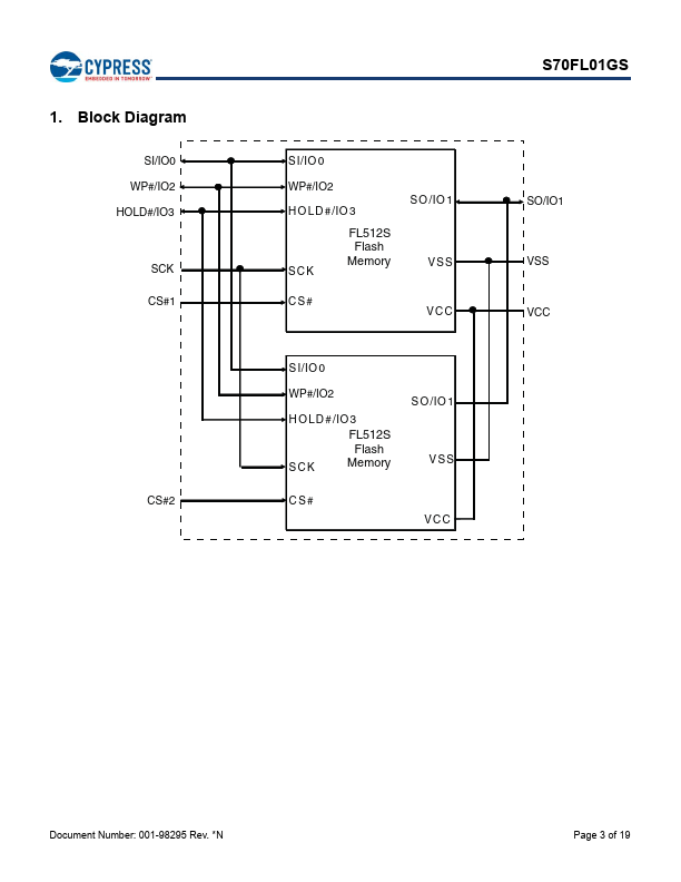
This document contains information for the S70FL01GS device, which is a dual die stack of two S25FL512S die. For detailed specifications, refer to the discrete die datasheet provided in the Affected Documents/Related Documents table. Affected Documents/Related Documents Document Title Publication Number S25FL512S 512 Mbit (64 Mbyte) 3.0V SPI Flash Memory Datasheet 001-98284 Cypress Semiconductor Corporation 198...
S70FL01GS Key Features
- CMOS 3.0V Core
- Serial Peripheral Interface (SPI) with Multi-I/O
- SPI Clock polarity and phase modes 0 and 3
- Double Data Rate (DDR) option
- Extended Addressing: 32-bit address
- Serial mand set and footprint patible with S25FL-A, S25FL-K, and S25FL-P SPI families
- Multi I/O mand set and footprint patible with S25FL-P SPI family
- READ mands
- Normal, Fast, Dual, Quad, Fast DDR, Dual DDR, Quad DDR
- AutoBoot