MTC5806AQ8 Description
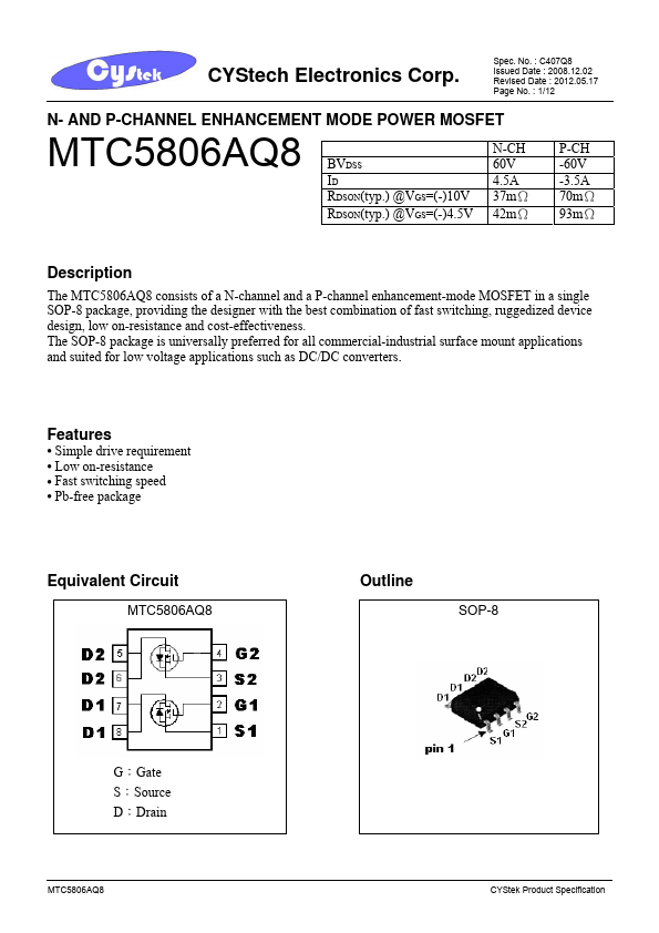
The MTC5806AQ8 consists of a N-channel and a P-channel enhancement-mode MOSFET in a single SOP-8 package, providing the designer with the best bination of fast switching, ruggedized device design, low on-resistance and cost-effectiveness. The SOP-8 package is universally preferred for all mercial-industrial surface mount applications and suited for low voltage applications such as DC/DC converters.
MTC5806AQ8 Key Features
- Simple drive requirement
- Low on-resistance
- Fast switching speed
- Pb-free package