Datasheet Summary
CYStech Electronics Corp.
Spec. No. : C407Q8 Issued Date : 2008.12.02 Revised Date : Page No. : 1/9
N- AND P-CHANNEL ENHANCEMENT MODE POWER MOSFET
Description
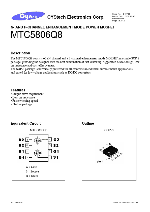
The MTC5806Q8 consists of a N-channel and a P-channel enhancement-mode MOSFET in a single SOP-8 package, providing the designer with the best bination of fast switching, ruggedized device design, low on-resistance and cost-effectiveness. The SOP-8 package is universally preferred for all mercial-industrial surface mount applications and suited for low voltage applications such as DC/DC converters.
Features
- Simple drive requirement
- Low on-resistance
- Fast switching speed
- Pb-free package
Equivalent...