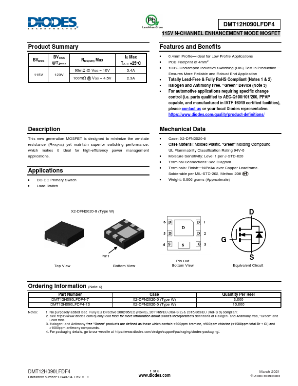
Datasheet Summary
Product Summary
BVDSS 115V
BVDSS @TJmax
120V
RDS(ON) Max 90mΩ @ VGS = 10V 100mΩ @ VGS = 4.5V
ID Max TA = +25°C
3.4A 2.3A
115V N-CHANNEL ENHANCEMENT MODE MOSFET
Features and Benefits
- 0.4mm Profile- Ideal for Low Profile Applications
- PCB Footprint of 4mm2
- 100% Unclamped Inductive Switching (UIS) Test in Production-
Ensures More Reliable and Robust End Application
- Totally Lead-Free & Fully RoHS pliant (Notes 1 & 2)
- Halogen and Antimony Free. “Green” Device (Note 3)
- For automotive applications requiring specific change control (i.e. parts qualified to AEC-Q100/101/200, PPAP capable, and manufactured in IATF 16949 certified facilities), please contact us or...