EMD11N15F
EMD11N15F is Single N-Channel Logic Level Enhancement Mode Field Effect Transistor manufactured by Excelliance MOS.
Single N-Channel Logic Level Enhancement Mode Field Effect Transistor
Product Summary:
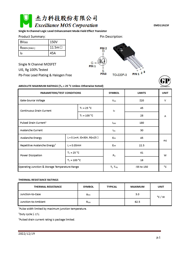
Pin Description:
BVDSS
150V
RDSON (MAX.)
11.5mΩ
45A
Single N Channel MOSFET UIS, Rg 100% Tested Pb-Free Lead Plating & Halogen...