Datasheet Details
| Part number | 74LCX16500 |
|---|---|
| Manufacturer | Fairchild Semiconductor (now onsemi) |
| File Size | 71.77 KB |
| Description | Low Voltage 18-Bit Universal Bus Transceivers |
| Datasheet |
 74LCX16500 Datasheet 74LCX16500 Datasheet
|
|
|
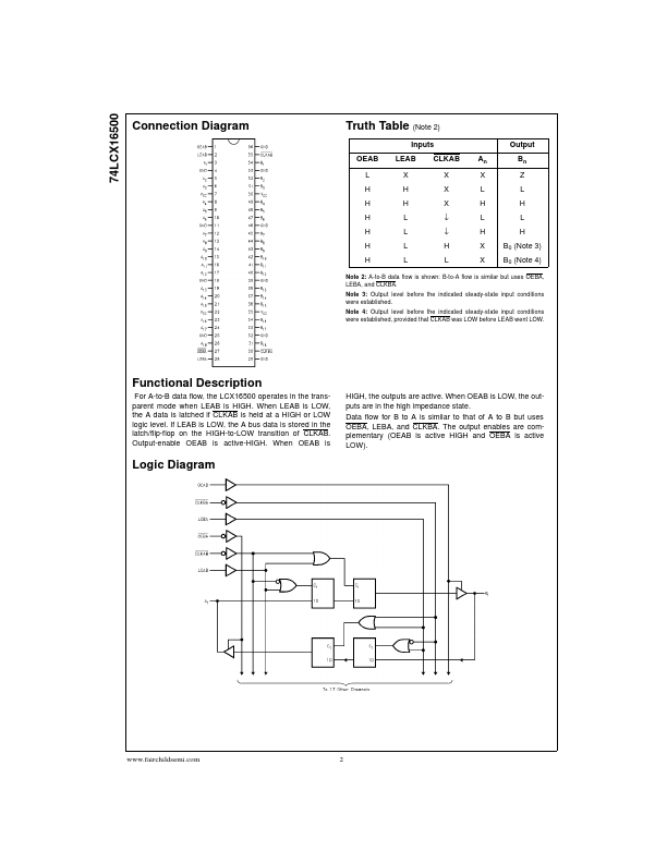
These 18-bit universal bus transceivers combine D-type latches and D-type flip-flops to allow data flow in transparent, latched, and clocked modes.
Data flow in each direction is controlled by output-enable (OEAB and OEBA), latch-enable (LEAB and LEBA), and clock (CLKAB and CLKBA) inputs.
| Part number | 74LCX16500 |
|---|---|
| Manufacturer | Fairchild Semiconductor (now onsemi) |
| File Size | 71.77 KB |
| Description | Low Voltage 18-Bit Universal Bus Transceivers |
| Datasheet |
74LCX16500 Datasheet
|
|
|
|