MC100ES60T22
Overview
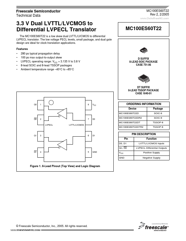
- 280 ps typical propagation delay 100 ps max output-to-output skew LVPECL operating range: VCC = 3.135 V to 3.8 V 8-lead SOIC and 8-lead TSSOP packages Ambient temperature range -40°C to +85°C
| Part | MC100ES60T22 |
|---|---|
| Description | 3.3 V Dual LVTTL/LVCMOS to Differential LVPECL Translator |
| Manufacturer | Freescale Semiconductor |
| Size | 117.90 KB |
| Part Number | Manufacturer | Description |
|---|---|---|
| HEF4104B | Nexperia | Quad low-to-high voltage translator |
| YF08E | Texas Instruments | Voltage Translator |
| SLA7061M | Allegro MicroSystems | UNIPOLAR STEPPER-MOTOR TRANSLATOR/DRIVERS |