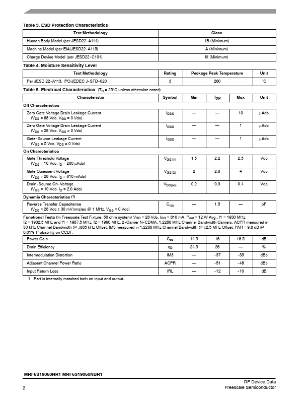
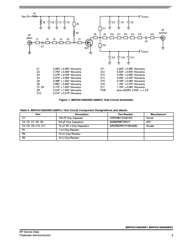
Datasheet4U Logo Datasheet4U.com

MRF6S19060NR1 - RF Power Field Effect Transistors

This page provides the datasheet information for the MRF6S19060NR1, a member of the MRF6S19060NBR1 RF Power Field Effect Transistors family.

Description

100 nF Chip Capacitor 6.8 pF Chip Capacitors 10 μF, 50 V Chip Capacitors 1 kW Chip Resistor 10 kW Chip Resistor 10 W Chip Resistor Part Number CDR33BX104AKWS 600B6R8BT250XT GRM55DR61H106KA88L Manufacturer Kemet ATC Murata MRF6S19060NR1 MRF6S19060NBR1 RF Device Data Freescale Semiconductor 3 R1 R2

Features

  • Characterized with Series Equivalent Large - Signal Impedance Parameters.
  • Internally Matched for Ease of Use.
  • Qualified Up to a Maximum of 32 VDD Operation.
  • Integrated ESD Protection.
  • Designed for Lower Memory Effects and Wide Instantaneous Bandwidth.

📥 Download Datasheet

Datasheet preview – MRF6S19060NR1
Other Datasheets by Freescale Semiconductor

Full PDF Text Transcription

Click to expand full text
www.DataSheet4U.com 
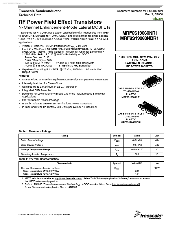
Freescale Semiconductor Technical Data Document Number: MRF6S19060N Rev. 3, 5/2006 RF Power Field Effect Transistors N - Channel Enhancement - Mode Lateral MOSFETs Designed for N - CDMA base station applications with frequencies from 1930 to 1990 MHz. Suitable for TDMA, CDMA and multicarrier amplifier applicat i o n s . To b e u s e d i n C l a s s A B f o r P C N - P C S / c e l l u l a r r a d i o a n d W L L applications. • Typical 2 - Carrier N - CDMA Performance: VDD = 28 Volts, IDQ = 610 mA, Pout = 12 Watts Avg., Full Frequency Band, IS - 95 CDMA (Pilot, Sync, Paging, Traffic Codes 8 Through 13) Channel Bandwidth = 1.2288 MHz. PAR = 9.8 dB @ 0.01% Probability on CCDF. Power Gain — 16 dB Drain Efficiency — 26% IM3 @ 2.5 MHz Offset — - 37 dBc in 1.
Published: |