Description
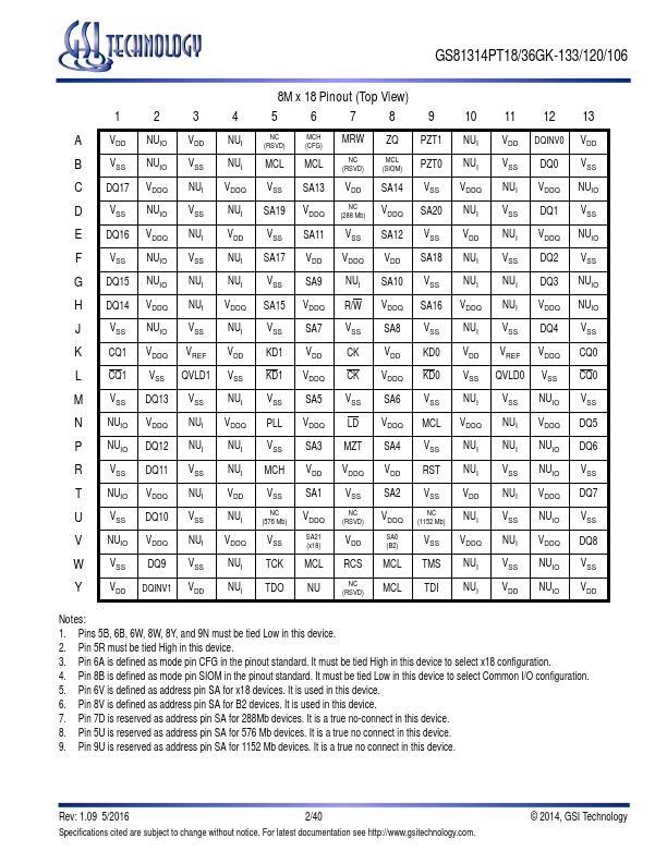
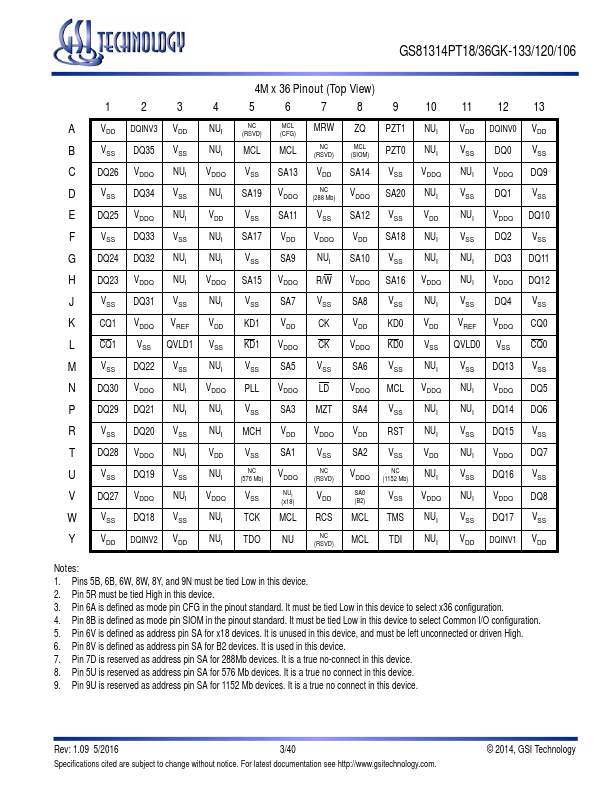
Symbol
Description
SA[21:0] DQ[35:0]
DQINV[3:0]
QVLD[1:0] CK, CK KD[1:0], KD[1:0] CQ[1:0], CQ[1:0] LD R/W MRW PLL RST ZQ RCS
Address
Read or write address is registered on CK.
Registered on KD and KD during Write operations; aligned with CQ and CQ during Read operations.
Registered on KD and KD (along with write data) during Write operations; indicate if the associated
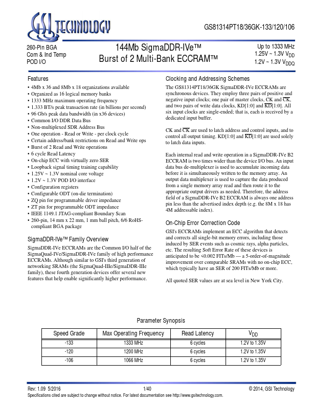
Features
- 4Mb x 36 and 8Mb x 18 organizations available.
- Organized as 16 logical memory banks.
- 1333 MHz maximum operating frequency.
- 1.333 BT/s peak transaction rate (in billions per second).
- 96 Gb/s peak data bandwidth (in x36 devices).
- Common I/O DDR Data Bus.
- Non-multiplexed SDR Address Bus.
- One operation - Read or Write - per clock cycle.
- Certain address/bank restrictions on Read and Write ops.
- Burst of 2 Read a.