Datasheet Summary
..
Pb Free Plating Product
ISSUED DATE :2005/05/06 REVISED DATE :
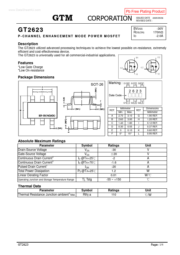
P-CHANNEL ENHANCEMENT MODE POWER MOSFET
BVDSS RDS(ON) ID
-30V 170m -2.0A
The GT2623 utilized advanced processing techniques to achieve the lowest possible on-resistance, extremely efficient and cost-effectiveness device. The GT2623 is universally used for all mercial-industrial applications.
Description
- Low Gate Charge
- Low On-resistance
Features
Package Dimensions
REF. A B C D E F
Millimeter Min. 2.70 2.60 1.40 0.30 0 0° Max. 3.10 3.00 1.80 0.55 0.10 10°
REF. G H I J K L
Dimensions Millimeter 1.90 REF. 1.20 REF. 0.12 REF. 0.37 REF. 0.60 REF. 0.95...