GTC9926
GTC9926 is N-CHANNEL ENHANCEMENT MODE POWER MOSFET manufactured by GTM.
..
Pb Free Plating Product
ISSUED DATE :2004/10/18 REVISED DATE :2006/07/27B
N-CHANNEL ENHANCEMENT MODE POWER MOSFET
BVDSS RDS(ON) ID
20V 28m 6A
Description
The GTC9926 provides the designer with the best bination of fast switching, ruggedized device design, ultra low on-resistance and cost-effectiveness.
- Low on-resistance
- Capable of 2.5V gate drive
- Low drive current
Features
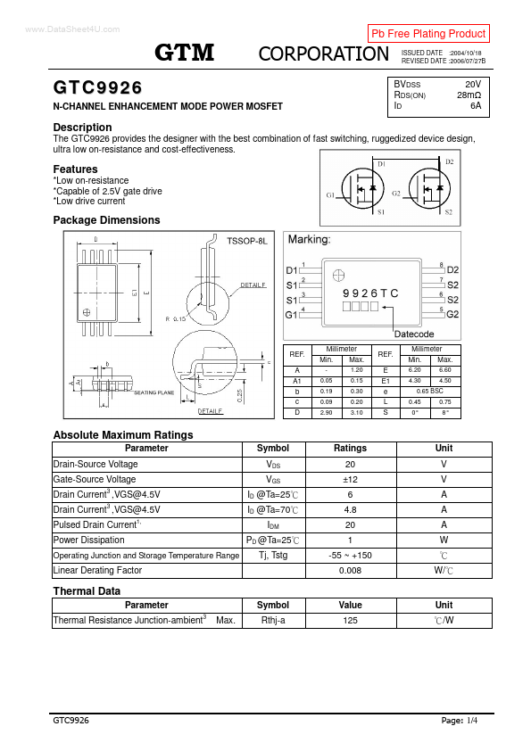
Package Dimensions
REF. A A1 b c D
Millimeter Min.
0.05 0.19 0.09 2.90
Max.
1.20 0.15 0.30 0.20 3.10
REF. E E1 e L S
Millimeter Min.
6.20 4.30 0.45 0°
Max.
6.60 4.50 0.75 8°
0.65...