GTC9922E
GTC9922E is N-CHANNEL ENHANCEMENT MODE POWER MOSFET manufactured by GTM.
Description
Features
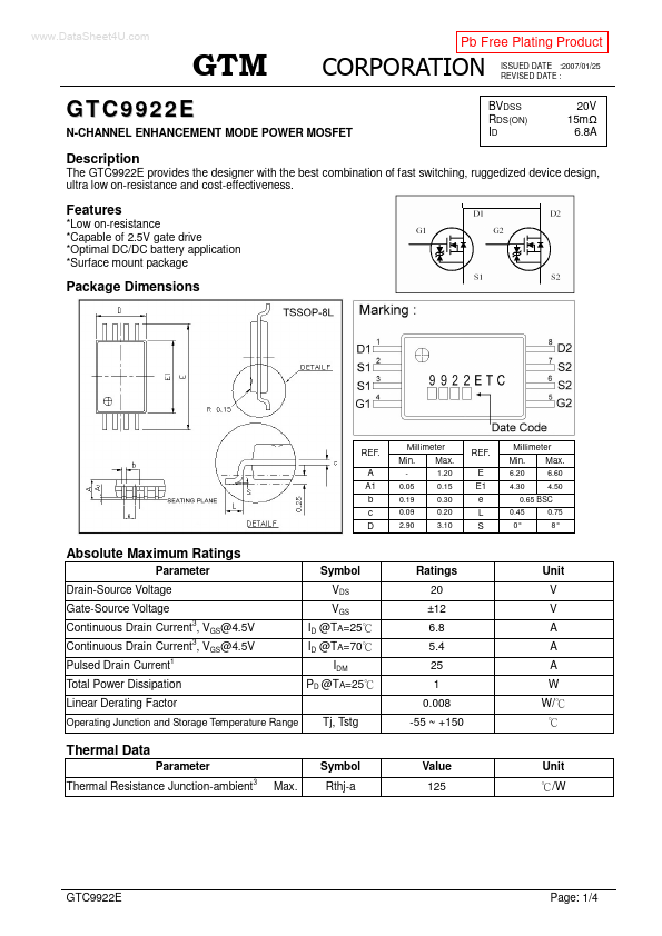
Package Dimensions
REF. A A1 b c D
Millimeter Min.
0.05 0.19 0.09 2.90
Max.
1.20 0.15 0.30 0.20 3.10
REF. E E1 e L S
Millimeter Min.
6.20 4.30 0.45 0°
Max.
6.60 4.50 0.75 8°
0.65 BSC
Absolute Maximum Ratings
Parameter Drain-Source Voltage Gate-Source Voltage Continuous Drain Current , VGS@4.5V Continuous Drain Current , VGS@4.5V Pulsed Drain Current
1 3 3
Symbol VDS VGS ID @TA=25 ID @TA=70 IDM PD @TA=25 Tj, Tstg
Ratings 20 ±12 6.8 5.4 25 1 0.008 -55 ~ +150
Unit V V A A A W W/
Total Power Dissipation Linear Derating Factor
Operating Junction and Storage Temperature Range
Thermal Data
Parameter Thermal Resistance Junction-ambient
Symbol Max. Rthj-a
Value 125
Unit /W
Page: 1/4
ISSUED DATE :2007/01/25 REVISED DATE :
Electrical Characteristics (Tj = 25
Parameter Drain-Source Breakdown Voltage
Breakdown Voltage Temperature Coefficient unless otherwise specified)
Min. 20 0.5 Typ. 0.05 22 25 3 9 11 12 47 23 1730 280 240 2.2 Max. 1.2 ±10 10 100 15 20 40 2770 p F ns n C Unit V V/ V S u A u A u A m Test Conditions VGS=0, ID=250u A Reference to 25 , ID=1m A VDS=VGS, ID=1m A VDS=4.5V, ID=6A VGS= ±12V VDS=20V, VGS=0 VDS=16V, VGS=0 VGS=4.5V, ID=6A VGS=2.5V, ID=4A ID=6A VDS=16V VGS=4.5V VDS=15V ID=1A VGS=4.5V RG=3.3 RD=15 VGS=0V VDS=20V f=1.0MHz f=1.0MHz
Symbol BVDSS
BVDSS / Tj
Gate Threshold Voltage Forward Transconductance Gate-Source Leakage Current
Drain-Source Leakage Current(Tj=25 ) Drain-Source Leakage Current(Tj=70 )
VGS(th) gfs IGSS IDSS
Static Drain-Source On-Resistance2 Total Gate...