Datasheet4U Logo Datasheet4U.com

GD25Q512 - Dual and Quad SPI Flash

Download the GD25Q512 datasheet PDF. This datasheet also covers the GD25Q40 variant, as both devices belong to the same dual and quad spi flash family and are provided as variant models within a single manufacturer datasheet.

📥 Download Datasheet

Note: The manufacturer provides a single datasheet file (GD25Q40-GigaDevice.pdf) that lists specifications for multiple related part numbers.

General Description

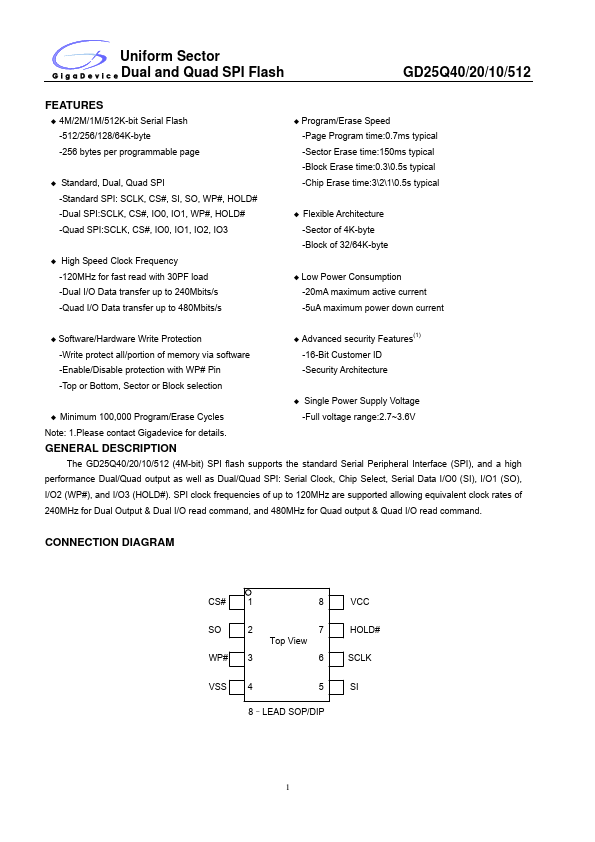
The GD25Q40/20/10/512 (4M-bit) SPI flash supports the standard Serial Peripheral Interface (SPI), and a high performance Dual/Quad output as well as Dual/Quad SPI: Serial Clock, Chip Select, Serial Data I/O0 (SI), I/O1 (SO), I/O2 (WP#), and I/O3 (HOLD#).

SPI clock frequencies of up to 120MHz are supported allowing equivalent clock rates of 240MHz for Dual Output & Dual I/O read command, and 480MHz for Quad output & Quad I/O read command.

CONNECTION DIAGRAM CS# 1 8 SO WP# 27 Top View 36 VSS 45 8–LEAD SOP/DIP VCC HOLD# SCLK SI 1 Uniform Sector Dual and Quad SPI Flash GD25Q40/20/10/512 PIN DESCRIPTION Pin Name I/O CS# I SO (IO1) I/O WP# (IO2) I/O VSS SI (IO0) I/O SCLK I HOLD# (IO3) I/O VCC Description Chip Select Input Data Output (Data Input Output 1) Write Protect Input (Da

Overview

Uniform Sector Dual and Quad SPI Flash GD25Q40/20/10/512.

Key Features

  • 4M/2M/1M/512K-bit Serial Flash -512/256/128/64K-byte -256 bytes per programmable page.
  • Standard, Dual, Quad SPI -Standard SPI: SCLK, CS#, SI, SO, WP#, HOLD# -Dual SPI:SCLK, CS#, IO0, IO1, WP#, HOLD# -Quad SPI:SCLK, CS#, IO0, IO1, IO2, IO3.
  • High Speed Clock Frequency -120MHz for fast read with 30PF load -Dual I/O Data transfer up to 240Mbits/s -Quad I/O Data transfer up to 480Mbits/s.
  • Program/Erase Speed -Page Program time:0.7ms typical -Sector Erase time:150ms typical -Bloc.