BFG540 Overview
Description
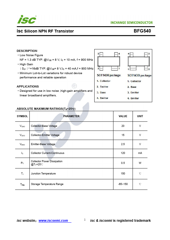
Low Noise Figure NF = 1.3 dB TYP. @VCE = 8 V, IC = 10 mA, f = 900 MHz - High Gain ︱S21︱2 =16dB TYP.
| Part | BFG540 |
|---|---|
| Description | SOT-143 Silicon NPN RF Transistor |
| Category | Transistor |
| Manufacturer | Inchange Semiconductor |
| Size | 244.53 KB |
Low Noise Figure NF = 1.3 dB TYP. @VCE = 8 V, IC = 10 mA, f = 900 MHz - High Gain ︱S21︱2 =16dB TYP.
| Part Number | Manufacturer | Description |
|---|---|---|
| BFG540 | Kexin Semiconductor | NPN 9GHz Wideband Transistor |
| BFG540 | EVVO | NPN Silicon Epitaxial Planar Transistor |
| BFG540 | NXP Semiconductors | NPN 9GHz wideband transistor |
| BFG540W | NXP Semiconductors | NPN 9 GHz wideband transistor |
| BFG540X | Philips Semiconductors | NPN 9 GHz wideband transistor |