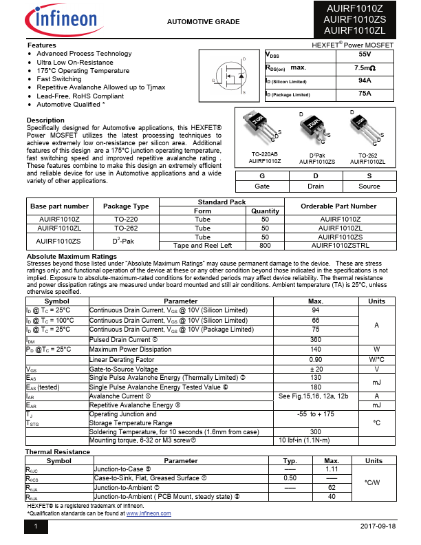
AUIRF1010Z/S/L
Static @ TJ = 25°C (unless otherwise specified)
Parameter
Min. Typ. Max. Units
Conditions
V(BR)DSS
Drain-to-Source Breakdown Voltage
V(BR)DSS/TJ Breakdown Voltage Temp. Coefficient
RDS(on)
Static Drain-to-Source On-Resistance
VGS(th)
Gate Threshold Voltage
gfs Forward Trans conductance
IDSS Drain-to-Source Leakage Current
IGSS
Gate-to-Source Forward Leakage
Gate-to-Source Reverse Leakage
55 ––– ––– V VGS = 0V, ID = 250µA
––– 0.049 ––– V/°C Reference to 25°C, ID = 1mA
––– 5.8 7.5 m VGS = 10V, ID = 75A
2.0 ––– 4.0 V VDS = VGS, ID = 250µA
33 ––– ––– S VDS = 25V, ID = 75A
–––
–––
–––
–––
20
250
µA
VDS = 55 V, VGS = 0V
VDS = 55V,VGS = 0V,TJ =125°C
–––
–––
––– 200
––– -200
nA
VGS = 20V
VGS = -20V
Dynamic Electrical Characteristics @ TJ = 25°C (unless otherwise specified)
Qg Total Gate Charge
Qgs Gate-to-Source Charge
Qgd Gate-to-Drain Charge
td(on) Turn-On Delay Time
tr Rise Time
td(off) Turn-Off Delay Time
tf Fall Time
LD Internal Drain Inductance
LS Internal Source Inductance
Ciss Input Capacitance
Coss Output Capacitance
Crss Reverse Transfer Capacitance
Coss Output Capacitance
Coss eff.
Effective Output Capacitance
Diode Characteristics
––– 63 95
––– 19 –––
––– 24 –––
––– 18 –––
––– 150 –––
––– 36 –––
––– 92 –––
––– 4.5 –––
––– 7.5 –––
––– 2840 –––
––– 420 –––
––– 250 –––
––– 1630 –––
––– 360 –––
––– 560 –––
ID = 75A
nC VDS = 44V
VGS = 10V
VDD = 28V
ns
ID = 75A
RG= 6.8
VGS = 10V
Between lead,
nH
6mm (0.25in.)
from package
and center of die contact
VGS = 0V
VDS = 25V
pF
ƒ = 1.0MHz, See Fig. 5
VGS = 0V, VDS = 1.0V ƒ = 1.0MHz
VGS = 0V, VDS = 44V ƒ = 1.0MHz
VGS = 0V, VDS = 0V to 44V
Parameter
IS
Continuous Source Current
(Body Diode)
ISM
Pulsed Source Current
(Body Diode)
VSD Diode Forward Voltage
trr Reverse Recovery Time
Qrr Reverse Recovery Charge
ton Forward Turn-On Time
Min. Typ. Max. Units
Conditions
––– ––– 75
––– ––– 360
MOSFET symbol
A
showing the
integral reverse
p-n junction diode.
––– ––– 1.3 V TJ = 25°C,IS = 75A,VGS = 0V
––– 22 33 ns TJ = 25°C ,IF = 75A, VDD = 25V
––– 15 23 nC di/dt = 100A/µs
Intrinsic turn-on time is negligible (turn-on is dominated by LS+LD)
Notes:
Repetitive rating; pulse width limited by max. junction temperature. (See fig. 11)
Limited by TJmax, starting TJ = 25°C, L = 0.05mH, RG = 25, IAS = 75A, VGS =10V. Part not recommended for use above this value.
Pulse width 1.0ms; duty cycle 2%.
Coss eff. is a fixed capacitance that gives the same charging time as Coss while VDS is rising from 0 to 80% VDSS.
Limited by TJmax , see Fig.12a, 12b, 15, 16 for typical repetitive avalanche performance.
This value determined from sample failure population, starting TJ = 25°C, L = 0.05mH, RG = 25, IAS = 75A, VGS =10V.
This is only applied to TO-220AB package.
When mounted on 1" square PCB (FR-4 or G-10 Material). For recommended footprint and soldering techniques refer to
application note #AN-994
R is measured at TJ approximately 90°C.
2 2017-09-18