ICS9112-27 Overview
Description
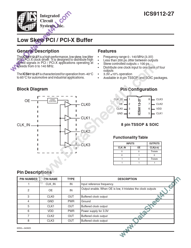
Input reference frequency. When OE is low, it tristates the clock outputs Buffered clock output Ground Buffered clock output Power supply for 3.3V Buffered clock output Buffered clock output w w w .D a S a t e e h U 4 t m o .c ICS9112-27 Supply voltage range VDD.