Datasheet Details
| Part number | ICS9112-26 |
|---|---|
| Manufacturer | Renesas |
| File Size | 614.28 KB |
| Description | Low Skew Output Buffer |
| Datasheet |
 ICS9112-26 Datasheet ICS9112-26 Datasheet
|
|
|
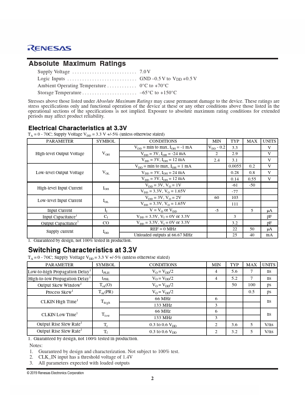
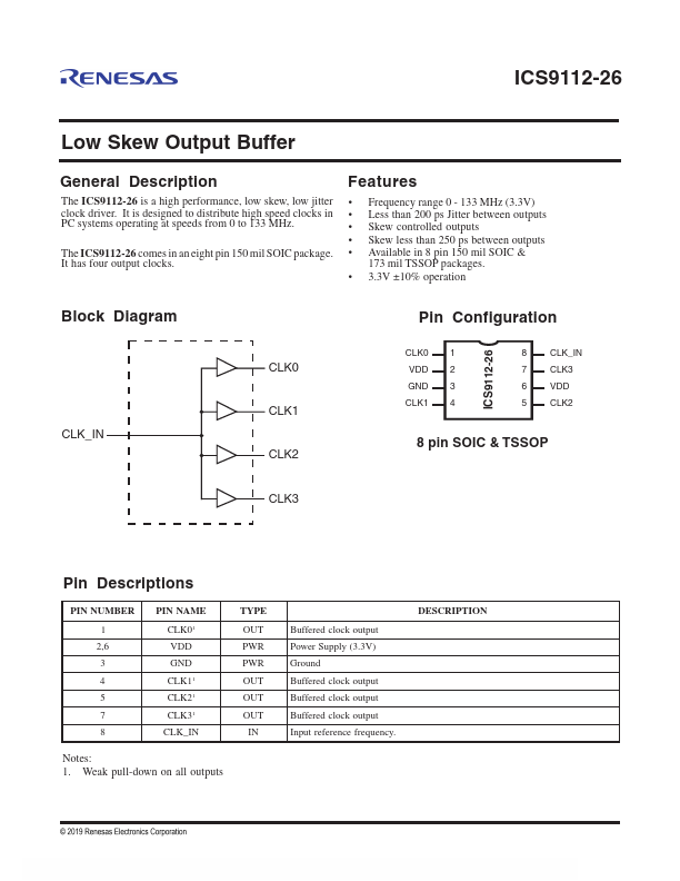
The ICS9112-26 is a high performance, low skew, low jitter clock driver.
It is designed to distribute high speed clocks in PC systems operating at speeds from 0 to 133 MHz.
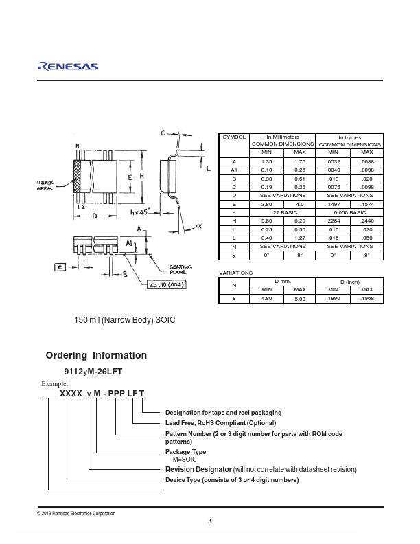
The ICS9112-26 comes in an eight pin 150 mil SOIC package.
| Part number | ICS9112-26 |
|---|---|
| Manufacturer | Renesas |
| File Size | 614.28 KB |
| Description | Low Skew Output Buffer |
| Datasheet |
ICS9112-26 Datasheet
|
|
|
|