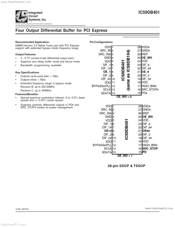
ICS9DB401 Overview
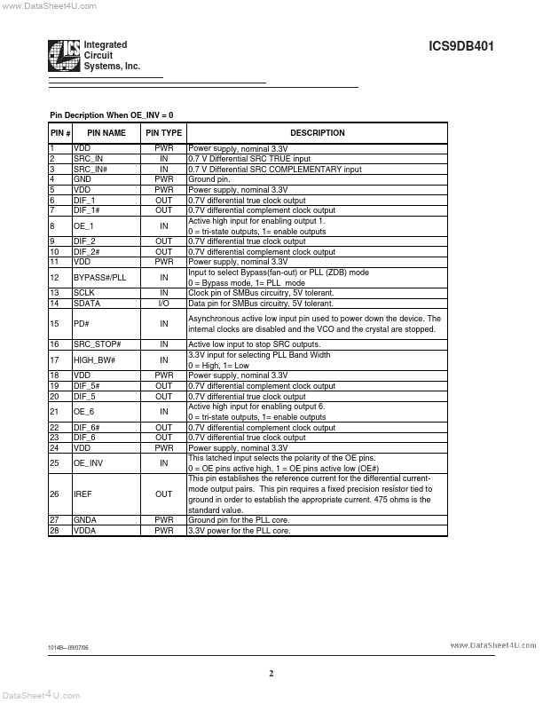
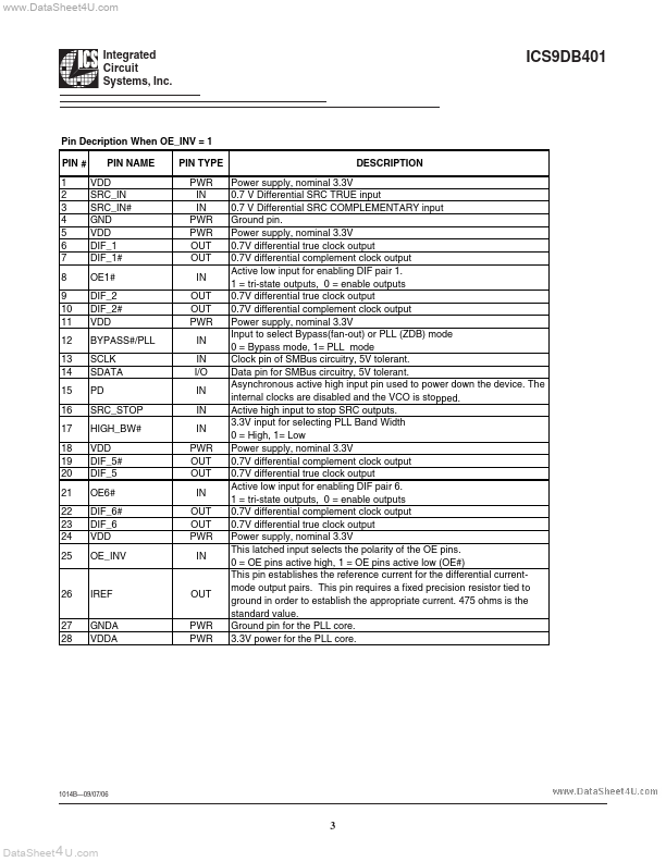
Power supply, nominal 3.3V 0.7 V Differential SRC TRUE input 0.7 V Differential SRC PLEMENTARY input Ground pin. Power supply, nominal 3.3V 0.7V differential true clock output 0.7V differential plement clock output Active high input for enabling output 1. 0 = tri-state outputs, 1= enable outputs 0.7V differential true clock output 0.7V differential plement clock output Power supply, nominal 3.3V Input to select...
ICS9DB401 Key Features
- 0.7V current-mode differential output pairs
- Supports zero delay buffer mode and fanout mode
- Bandwidth programming available Key Specifications
- Outputs cycle-cycle jitter: < 50ps
- Outputs skew: < 50ps
- Extended frequency range in bypass mode: Revision B: up to 333.33MHz Revision C: up to 400MHz Features/Benefits
- Spread spectrum modulation tolerant, 0 to -0.5% down spread and +/- 0.25% center spread
- Supports undriven differential outputs in PD# and SRC_STOP# modes for power management