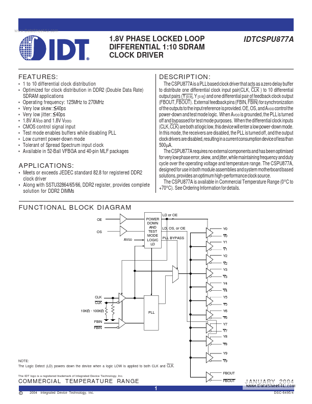
Datasheet4U Logo Datasheet4U.com

IDTCSPU877A Datasheet 1.8V PHASE LOCKED LOOP DIFFERENTIAL 1:10 SDRAM CLOCK DRIVER

Manufacturer: Integrated Device Technology

Datasheet Details

Part number IDTCSPU877A
Manufacturer Integrated Device Technology
File Size 179.31 KB
Description 1.8V PHASE LOCKED LOOP DIFFERENTIAL 1:10 SDRAM CLOCK DRIVER
Download IDTCSPU877A Download (PDF)

General Description

: IDTCSPU877A • 1 to 10 differential clock distribution • Optimized for clock distribution in DDR2 (Double Data Rate) SDRAM applications • Operating frequency: 125MHz to 270MHz • Very low skew: ≤40ps • Very low jitter: ≤40ps • 1.8V AVDD and 1.8V VDDQ • CMOS control signal input • Test mode enables buffers while disabling PLL • Low current power-down mode • Tolerant of Spread Spectrum input clock • Available in 52-Ball VFBGA and 40-pin MLF packages APPLICATIONS: • Meets or exceeds JEDEC standard 82.8 for registered DDR2 clock driver • Along with SSTU32864/65/66, DDR2 register, provides complete solution for DDR2 DIMMs The CSPU877A is a PLL based clock driver that acts as a zero delay buffer to distribute one differential clock input pair(CLK, CLK ) to 10 differential output pairs (Y [0:9], Y [0:9]) and one differential pair of feedback clock output (FBOUT, FBOUT).

External feedback pins (FBIN, FBIN) for synchronization of the outputs to the input reference is provided.

OE, OS, and AVDD control the power-down and test mode logic.

Overview

www.DataSheet4U.com IDTCSPU877A 1.8V PLL DIFFERENTIAL 1:10 SDRAM CLOCK DRIVER COMMERCIAL TEMPERATURE RANGE 1.