The following content is an automatically extracted verbatim text
from the original manufacturer datasheet and is provided for reference purposes only.
View original datasheet text
IS42S81600A, IS42S16800A, IS42S32400A,
16Meg x 8, 8Meg x16 & 4Meg x 32 128-MBIT SYNCHRONOUS DRAM
FEATURES
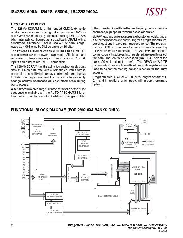
• Clock frequency: 166,143,100 MHz • Fully synchronous; all signals referenced to a positive clock edge • Internal bank for hiding row access/precharge • Power supply IS42S81600A IS42S16800A IS42S32400A • LVTTL interface • Programmable burst length – (1, 2, 4, 8, full page) • Programmable burst sequence: Sequential/Interleave • Auto Refresh (CBR) • Self Refresh with programmable refresh periods • 4096 refresh cycles every 64 ms • Random column address every clock cycle • Programmable CAS latency (2, 3 clocks) • Burst read/write and burst read/single write operations capability • Burst termination by burst stop and precharge command • Industrial Temperature Availability • Lead-free Avai
 42S16800A Datasheet