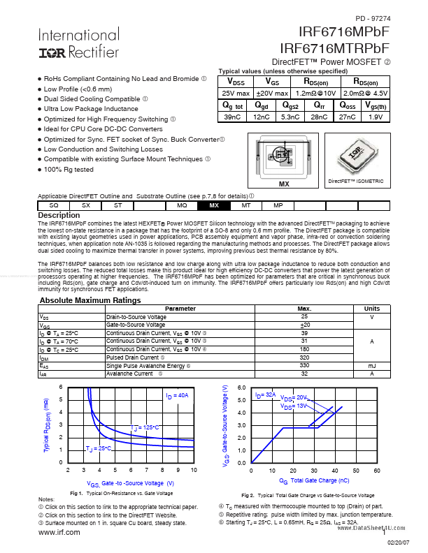
Datasheet4U Logo Datasheet4U.com

IRF6716MPBF Datasheet N-Channel HEXFET Power MOSFET

Manufacturer: International Rectifier (now Infineon)

Download the IRF6716MPBF datasheet PDF. This datasheet also includes the IRF6716MTRPBF variant, as both parts are published together in a single manufacturer document.

📥 Download Datasheet

Note: The manufacturer provides a single datasheet file (IRF6716MTRPBF_InternationalRectifier.pdf) that lists specifications for multiple related part numbers.

General Description

The IRF6716MPbF combines the latest HEXFET® Power MOSFET Silicon technology with the advanced DirectFETTM packaging to achieve the lowest on-state resistance in a package that has the footprint of a SO-8 and only 0.6 mm profile.

The DirectFET package is compatible with existing layout geometries used in power applications, PCB assembly equipment and vapor phase, infra-red or convection soldering techniques, when application note AN-1035 is followed regarding the manufacturing methods and processes.

The DirectFET package allows dual sided cooling to maximize thermal transfer in power systems, improving previous best thermal resistance by 80%.

Overview

IRF6716MPbF IRF6716MTRPbF l l l l l l l l l l PD - 97274 RoHs Compliant Containing No Lead and Bromide  VDSS VGS RDS(on) RDS(on) Low Profile (<0.6 mm) 25V max ±20V max 1.2mΩ@10V 2.0mΩ@ 4.5V Dual Sided Cooling Compatible  Qg tot Qgd Qgs2 Qrr Qoss Vgs(th) Ultra Low Package Inductance 39nC 12nC 5.3nC 28nC 27nC 1.9V Optimized for High Frequency Switching  Ideal for CPU Core DC-DC Converters Optimized for Sync.

FET socket of Sync.

Buck Converter Low Conduction and Switching Losses Compatible with existing Surface Mount Techniques  100% Rg tested MX DirectFET™ ISOMETRIC Typical values (unless otherwise specified) DirectFET™ Power MOSFET ‚ Applicable DirectFET Outline and Substrate Outline (see p.

Key Features

  • Voltage (V) 1 T A = 25°C T J = 150°C 0.1 0.01 Single Pulse 0.10 1.00 10.00 100.00 VDS, Drain-to-Source Voltage (V) Fig 10. Typical Source-Drain Diode Forward Voltage 40 35 30 25 20 15 10 5 0 25 50 75 100 125 150 T C , Case Temperature (°C) Fig 11. Maximum Safe Operating Area 3.0 Typical VGS(th) Gate threshold Voltage (V) 2.5 ID, Drain Current (A) 2.0 ID = 100µA ID = 250µA www. DataSheet4U. com 1.5 ID = 1.0mA ID = 1.0A 1.0 -75 -50 -25 0 25 50 75 100 125 150 T J , Temperature ( °C ).