The following content is an automatically extracted verbatim text
from the original manufacturer datasheet and is provided for reference purposes only.
View original datasheet text
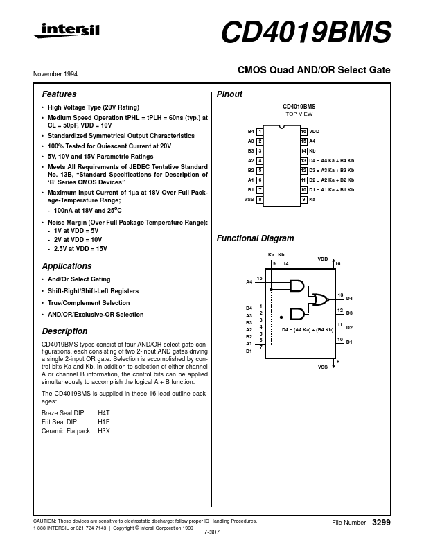
CD4019BMS
November 1994
CMOS Quad AND/OR Select Gate
Pinout
CD4019BMS TOP VIEW
B4 1 A3 2 B3 3 A2 4 B2 5 A1 6 B1 7 VSS 8 16 VDD 15 A4 14 Kb 13 D4 = A4 Ka + B4 Kb 12 D3 = A3 Ka + B3 Kb 11 D2 = A2 Ka + B2 Kb 10 D1 = A1 Ka + B1 Kb 9 Ka
Features
• High Voltage Type (20V Rating) • Medium Speed Operation tPHL = tPLH = 60ns (typ.) at CL = 50pF, VDD = 10V • Standardized Symmetrical Output Characteristics • 100% Tested for Quiescent Current at 20V • 5V, 10V and 15V Parametric Ratings • Meets All Requirements of JEDEC Tentative Standard No.
 CD4019BMS Datasheet