Part number:
CJAB35P03
Manufacturer:
JCET
File Size:
1.48 MB
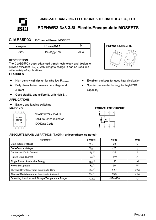
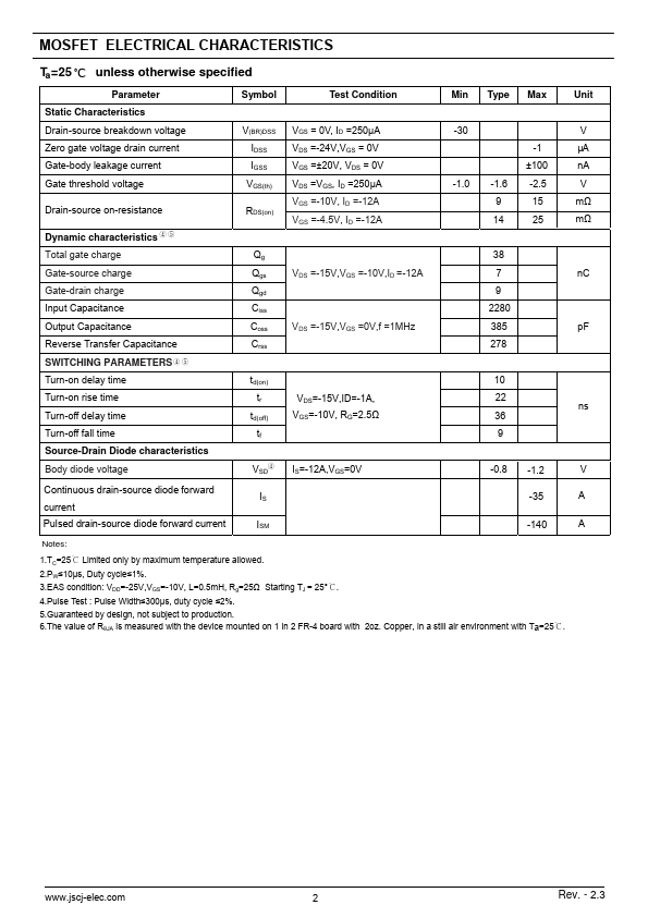
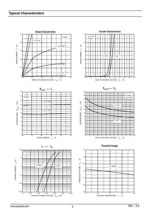
Description:
P-channel power mosfet.
CJAB35P03 Features
* High density cell design for ultra low RDS(ON)
* Fully characterized avalanche voltage and current
* Good stability and uniformity with high EAS APPLICATIONS
* Battery and loading switching MARKING CJAB 35P03 XX CJAB35P03 = Part No. Solid dot=Pin1 indicator XX=Date Code
* E
Datasheet Details
CJAB35P03
JCET
1.48 MB
P-channel power mosfet.
📁 Related Datasheet
CJAB35N03 N-Channel MOSFET (JCET)
CJAB25N03 N-Channel MOSFET (JCET)
CJA03N10 N-Channel MOSFET (JCET)
CJA03N10-HF N-Channel MOSFET (Comchip)
CJA1117-1.5 1A LOW DROPOUT LINEAR REGULATOR (Jiangsu Changjiang)
CJA1117-1.8 1A LOW DROPOUT LINEAR REGULATOR (Jiangsu Changjiang)
CJA1117-2.5 1A LOW DROPOUT LINEAR REGULATOR (Jiangsu Changjiang)
CJA1117-3.3 1A LOW DROPOUT LINEAR REGULATOR (Jiangsu Changjiang)
CJAB35P03 Distributor