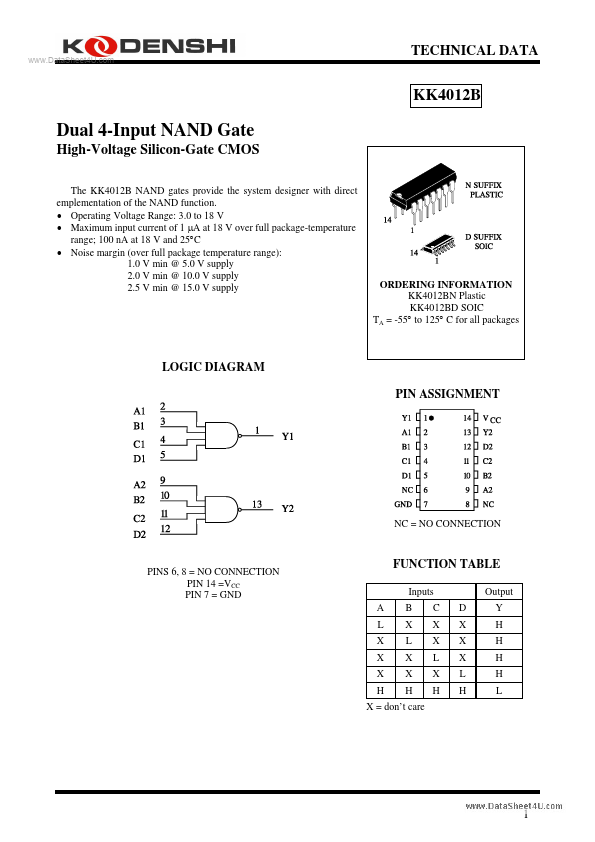
The following content is an automatically extracted verbatim text
from the original manufacturer datasheet and is provided for reference purposes only.
View original datasheet text
www.DataSheet4U.com
TECHNICAL DATA
KK4012B
Dual 4-Input NAND Gate
High-Voltage Silicon-Gate CMOS
The KK4012B NAND gates provide the system designer with direct emplementation of the NAND function. • Operating Voltage Range: 3.0 to 18 V • Maximum input current of 1 µA at 18 V over full package-temperature range; 100 nA at 18 V and 25°C • Noise margin (over full package temperature range): 1.0 V min @ 5.0 V supply 2.0 V min @ 10.0 V supply 2.5 V min @ 15.0 V supply
ORDERING INFORMATION KK4012BN Plastic KK4012BD SOIC TA = -55° to 125° C for all packages
LOGIC DIAGRAM PIN ASSIGNMENT
NC = NO CONNECTION
PINS 6, 8 = NO CONNECTION PIN 14 =VCC PIN 7 = GND A L X X X H
FUNCTION TABLE
Inputs B X L X X H C X X L X H D X X X L H Output Y H H H H L
X = don’t care
1
www.DataSheet4U.